Table 22: pll pins and their connections – Achronix Speedster22i HD1000 Development Kit User Guide User Manual
Page 54

54
UG034, July 1, 2014
Signal Name
Pin on HD1000 (U33)
Pin on ICS853310 (U72)
INTERLAKEN1_CLK2_P
AY32
20
INTERLAKEN1_CLK2_N
AW32
19
INTERLAKEN1_CLK3_P
BC31
18
INTERLAKEN1_CLK3_N
BB31
17
INTERLAKEN1_CLK4_P
AY31
16
INTERLAKEN1_CLK4_N
AW31
14
INTERLAKEN1_CLK5_P
BC29
13
INTERLAKEN1_CLK5_N
BB29
12
INTERLAKEN1_CLK6_P
BC28
11
INTERLAKEN1_CLK6_N
BB28
10
The 16 MHz oscillator (Y4) provides the clock to the microcontroller (U35).
The 25 MHz (Y7) crystal provides the input to the IDT 9FG430 Frequency Timing Generator
(U101). One of the 4 HCSL differential output pairs provides one of the input pairs to the IDT
IDT5V41068APGGI device (U57). The other input pair to U57 is (PCIE0_REFCLK_P
PCIE0_REFCLK_N). The output from the U57 device is selected by the CLK_SEL signal
(SW11) to support the PCIe interface.
There are four PLLs on the HD1000. These are designated PLL North West, PLL South West,
PLL South East and PLL North East.
PLL North West and PLL North East are used with the FMC connector. PLL South West
provides the clock circuitry for the PCIe connections. PLL South East uses a 16 MHz oscillator
(Y3) to drive the clocks on the SMA connectors J49 and J50.
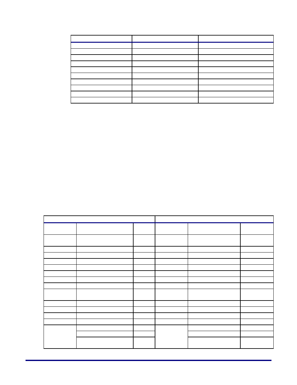
Table 22 shows the PLLs and their connections.
Table 22: PLL Pins and their Connections
PLL (U33)
Connection
Location
Pin Name
Pin
Through
Signal Name
Pin /
Component
North West
PAD0_CLK_BANK_NW
BC14
J3: FMC
Connector
CLK0_M2C_P
H5
PAD1_CLK_BANK_NW
BB14
CLK0_M2C_N
H4
PAD2_CLK_BANK_NW
BA14
CLK1_M2C_P
G3
PAD3_CLK_BANK_NW
AY14
CLK1_M2C_N
G2
PAD4_CLK_BANK_NW
AW14
CLK2_M2C_P
K5
PAD5_CLK_BANK_NW
AV14
CLK2_M2C_N
K4
North East
PAD0_CLK_BANK_NE
AW38
U99
FPGA_CLK_NW_P
3
PAD1_CLK_BANK_NE
AV37
FPGA_CLK_NW_N
4
PAD4_CLK_BANK_NE
AY38
J3: FMC
Connector
CLK3_M2C_P
J3
PAD5_CLK_BANK_NE
AW37
CLK3_M2C_N
J2
South West
PAD0_CLK_BANK_SW
P19
U99
FPGA_CLK_SW_P
1
PAD1_CLK_BANK_SW
P18
FPGA_CLK_SW_N
2
PAD4_CLK_BANK_SW
P15
U103
PCIE0_PERSTn_LT
4
South East
PAD0_CLK_BANK_SE
N38
HD1000
(U33)
J49 (SMA)
PAD1_CLK_BANK_SE
P37
J50 (SMA)
PAD2_CLK_BANK_SE
P38
Y3 (16 MHz
Osc.)
