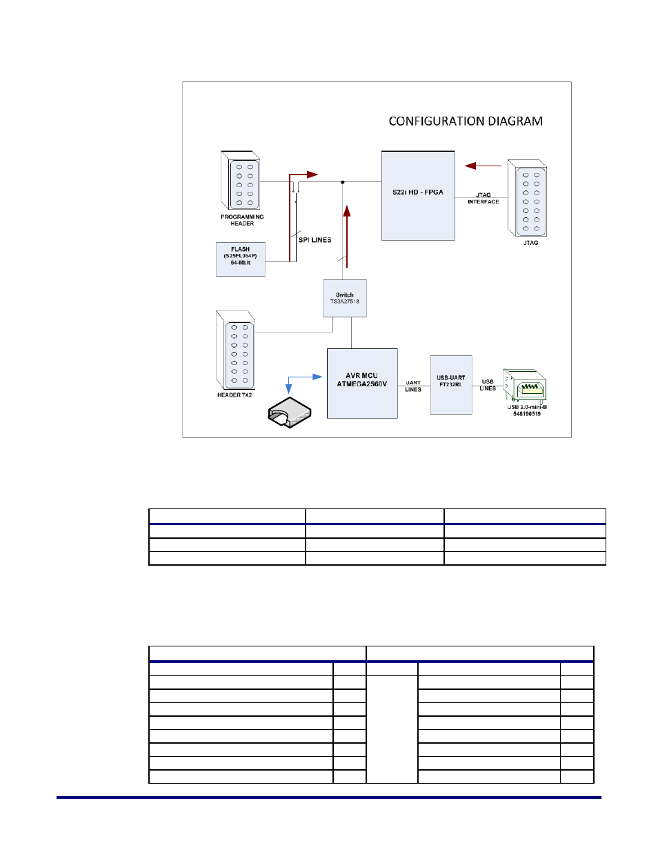
Table 1, Table 1. figure 8 – Achronix Speedster22i HD1000 Development Kit User Guide User Manual
Page 22

22
UG034, July 1, 2014
CPU x8 Mode
Programming
SPI Flash
Programming
SD CARD
JTAG
Programming
Figure 8: ACX-BRD-HD1000-100G Board Configuration Modes
Table 1: ACX-BRD-HD1000-100G Board Configuration Mode (J31)
Shunt Position
Configuration Mode
Bitstream Source
OPEN
JTAG
Development PC
2 & 4
Serial
FLASH
2 & 3
CPU
MicroSD
Table 2 shows the FPGA configuration pins for the all the modes and their connections.
Table 2: HD1000 Configuration Mode Pins and their Connections
HD1000 (U33)
Connection
Signal Name
Pin
Through Signal Name
Pin
CONFIG_MODESEL0
L17
SW7
CFG_MS0
1
CONFIG_MODESEL1
L18
CFG_MS1
2
CONFIG_MODESEL2
J17
CFG_MS2
3
CONFIG_SYS_CLK_BYPASS
N18
SCLK_BYP
4
CONFIG_CLKSEL
M17
CFG_CLKSL
5
PROGRAM_ENABLE0
K15
PRG_EN0
6
PROGRAM_ENABLE1
M19
PRG_EN1
7
STAP_SEL
L19
STAP_SEL
8
