Chapter 5, Clocking, Table 19: crystals/oscillators on the board – Achronix Speedster22i HD1000 Development Kit User Guide User Manual
Page 52: Sdk1000 clocking, Chapter 5 – clocking
52
UG034, July 1, 2014
Chapter 5
– Clocking
In this chapter you will learn about the crystals and oscillators on the board. These provide
the inputs to the clock synthesizers or the HD1000 clock banks to generate all the frequencies
required to implement the system level functions. You can also drive some of the clocks from
external sources using the relevant interface or through the SMA connectors.
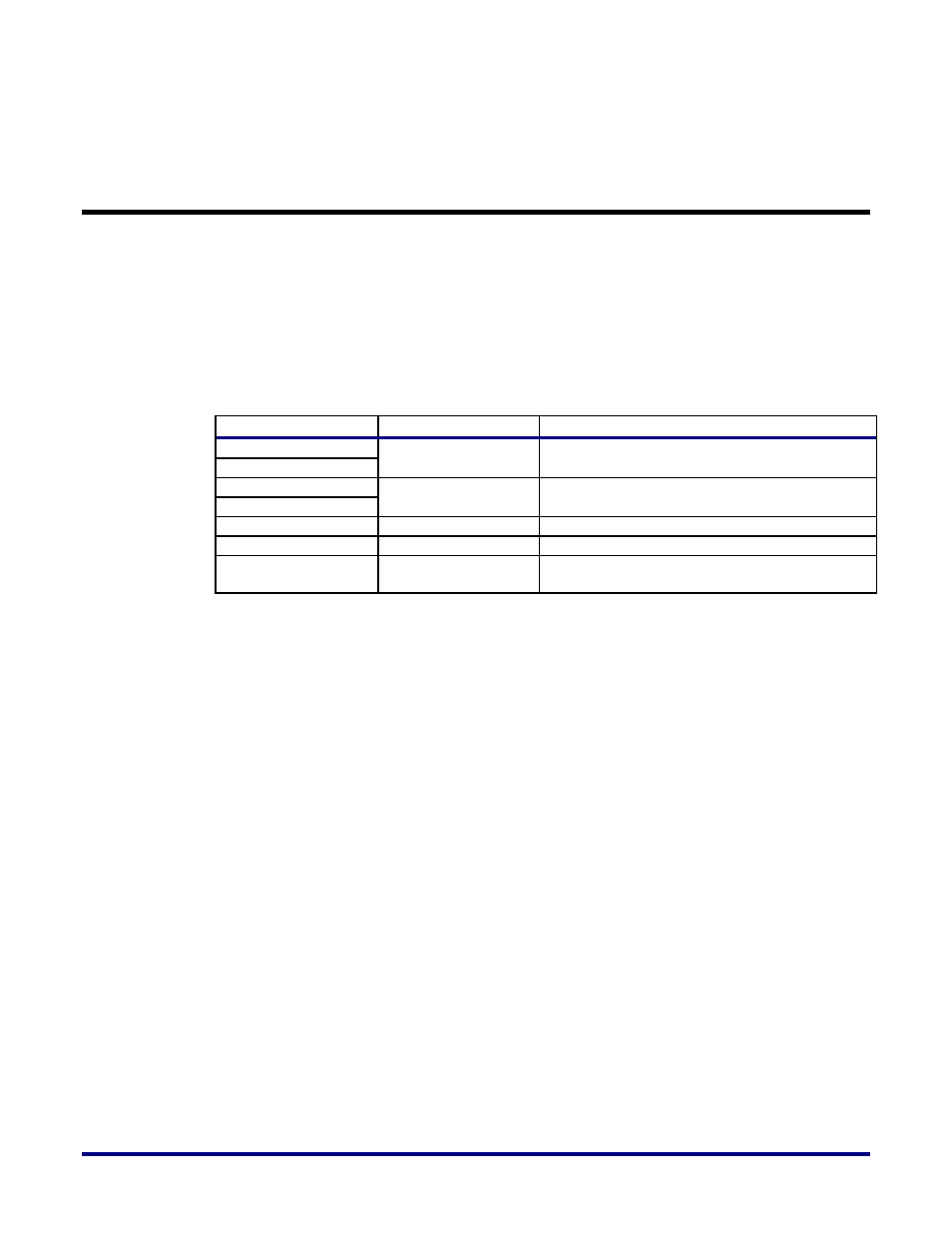
Table 19 shows all the crystals on the board and their functions.
Table 19: Crystals/Oscillators on the Board
Crystal/Oscillator
Frequency (MHz)
Function
Y6
25
Banks NW & SW (20
– 600 MHz, LVDS)
Y5
Y2
25
Clocks for Interlaken-1 Clock synthesizer,
SerDes North (30
– 350 MHz LVPECL)
Y1
Y4
16
Microcontroller Clock
Y7
25
PCIe Clock
Y3
16
Drives PLL_CLK_16MHz input to HD1000
(PLL South East, Pin P38)
You can use the seven crystals on the board to synthesize all the reference clocks for the
system. Four of these (Y6, Y5, Y2, and Y1) are connected to IDT Femtoclock, ICS843034
devices (U102 and U19). The multipliers of these clock synthesizers can be dynamically
adjusted using DIP switches: SW1/2/5 for U19 and SW12/13/14 for U102 respectively.
U102 provides 20 – 600 MHz LVDS outputs that are used by the North East and South West
HD1000 FPGA General Purpose IO (GPIO) Banks. This clock synthesizer’s DIP switches are
configured by default to produce a 100MHz clock as input to the GPIOs. While the clock
synthesizer has a large output clock frequency range, it is recommended that the synthesizer
generate a frequency in the 62.5MHz to 200MHz range, and that a PLL internal to the FPGA
be used to further multiply, clean or introduce phase offset to generate a clock that will
ultimately be used to feed the FPGA fabric. Table 20 below highlights a set of predetermined
DIP switch settings that can be used to have the clock synthesizer produce the desired output
clock frequency to feed the FPGA.
Bear in mind that the clock synthesizer generates a differential clock signal that needs to be
terminated at the pad using a 100Ohm resistor. So the correct macro to use for an incoming
differential clock from the synthesizer to output a single ended clock which would then be
fed into a PLL or to the clock network and fabric, would look something like the following:
IPAD_DIFF #(
.odt(“on”),
.termination(“100”)
) synth_clk_pad (
.pad(synth_clk_p),
.padn(synth_clk_n),
.dout(synth_clk)
);