3 power supply voltage test – Tweco 400 MST Arc Master User Manual
Page 49

400MST
9
ADVANCED TROUBLESHOOTING
9 – 12
calculated measurement is not within the cor-
responding range (260~360/580~720VDC) fol-
lowing the process in section 9.2.4.23.
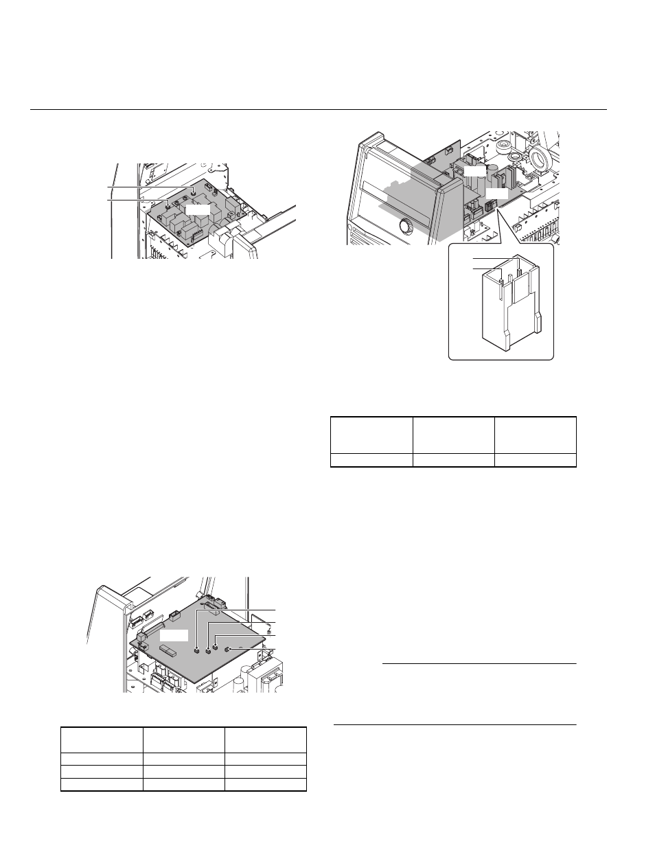
Figure 9-3: The check points TB1(P) and TB4(N)
7) After the replacement of D1, if the above volt-
age is still abnormal, replace PCB1 (WK-
5493).
1.4.3 Power Supply Voltage Test
Connect the power supply to a source of rated
input voltage. (Check the name plate on the rear of
the power supply for the proper input voltage.)
Apply power to the unit and place the switch of the
power supply to the ON position.
On the PCB6 (WK-5549) and PCB3 (WK-5548),
measure the voltages according to the following
table. The test point and the reference are obtain-
able on the parts side of PCB6 (WK-5549) and
PCB3 (WK-5548).
The location of points TP0-3 are indicated in Figure
9-4.
The location of points PIN1-PIN3 of CN18 on
PCB3 are indicated in Figure 9-5.
Figure 9-4: The check points TP0-3
Figure 9-5: The check points PIN1-PIN3 of CN18 on
PCB3
If any of these voltages are not present or are
below a 10% tolerance, replace PCB3 (WK-5548).
1.4.4 Verification of the Cooling Fan,
FAN1, Drive Circuitry
Verify the condition of the cooling fan, FAN1, using
a DC voltmeter. (The capability of the voltmeter
should be more than 50VDC.)
Using a DC voltmeter, measure between PIN 1[+]
and PIN 2[-] of CN11 on PCB3 (WK-5548).
The location of connector CN11 of PCB3 (WK-
5548) is indicated in Figure 9-6.
NOTE
When you measure the above voltage, do not
remove the connector. Conduct the measurement
while the connector plug and receptacle are still
connected.
Test Point
(PCB6;WK-5688)
Reference
(PCB6;WK-5688)
ACCEPTABLE
VALUE
TP1
TP0
+15VDC
TP2
TP0
+5VDC
TP3
TP0
–15VDC
PCB2
TB1(P)
TB4(N)
TP1
TP2
TP3
TP0
PCB6
Test Point
(CN18 on PCB3;
WK-5548)
Reference
(CN18 on PCB3;
WK-5548)
ACCEPTABLE
VALUE
PIN1
PIN3
+24VDC
PCB3
CN18
PIN 3
PIN 1
