SHIMPO DT-601CG User Manual
Page 47
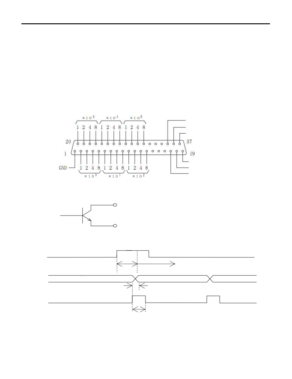
17. BCD OUTPUT
1. BCD code is all-digit parallel output at NPN open collector pulse output (DC30V 10mA MAX).
2. Output logic of data can be changed.(Refer to P40)
Positive Logic
: The collector of output transistor and emitter are conducting.
Negative Logic
: The collector of output transistor and emitter are not conducting.
3. Take data when TI signals to turning off.
logic of TI signal can be changed.(Refer to P40)
4. When this option is selected, D-sub37P male connector (XM2A-3701) and Hood (XM2S-3711) are attached
by the addition.
BCD Output Pin Layout (D-Sub 37P fenmale connector at meter side)
BCD Output Circuit Diagram (NPN open collector pulse output)
BCD Output Time Chart
Minus Sign
Decimal Point
TI Signal
Parity Output
REQ Input
GND
Meter side
Pin 2-13, 18-19, 20-31, 35-37 (DC30V, 10mA)
Pin 1, 17 (GND)
Request Signal
BCD Output Data
TI Signal
Data
Data
Data
25ms
Max. 10ms
Data is defined
P48
- DT-361 (36 pages)
- DT-365E (28 pages)
- DT-311A (4 pages)
- DT-311J (12 pages)
- DT-315AEB (4 pages)
- DT-315P (17 pages)
- DT-326 (35 pages)
- DT-725 (4 pages)
- DT-900 (33 pages)
- ST-1000 (2 pages)
- ST-5000 (4 pages)
- SG-300 (2 pages)
- DT-721 (4 pages)
- DT-329 (32 pages)
- DT-105A (2 pages)
- DT-107A (2 pages)
- MT-100 (4 pages)
- MT-200 (4 pages)
- PT-110 (2 pages)
- DT-105A-S12 (2 pages)
- DT-205L (4 pages)
- DT-205L-S12 (4 pages)
- DT-207L (4 pages)
- DT-207L-S12 (4 pages)
- DT-209X (68 pages)
- DT-5TXR (20 pages)
- DT-5RL-1 (2 pages)
- DT-5TP (8 pages)
- FGV-XY-Series (32 pages)
- FGE-X (8 pages)
- FGE-HX (8 pages)
- FG-3000 (8 pages)
- FG-7000-Series (8 pages)
- DFS-series (20 pages)
- DRI-series (20 pages)
- EM-series (2 pages)
- FGE-series (4 pages)
- FGV-series (4 pages)
- FGE-H-series (4 pages)
- FGV-H-series (4 pages)
- MF Series (2 pages)
- MFD_Series (2 pages)
- FGS-100E (20 pages)
- FGS-100-PXH (20 pages)