Anritsu 682XXB User Manual
Page 35

A14
SDM, SQM
Driver
A9
PIN
Control
10 MHz
HI-STAB
XTAL OSC
(Option)
10 MHz REF OUT
Real Panel BNC
Serial Data
10 MHz REF IN
Rear Panel BNC
0.01 - 2 GHz
RF Output
0.01 - 40 GHz
A3
Reference
Loop
A4
Coarse
Loop
A5
Fine
Loop
A7
YIG
Loop
21.5 - 40 MHz
Sampled
2 - 20 GHz
RF
YIG Loop Error
Serial Data
Serial Data
A11 FM
Serial Data
A13
YIG
Driver
A12
Analog
Instruction
A6
Pulse
Generator
FM
Main
Bias
Freq Band
Select (To A14)
110 dB
Step
Attenuator
(Option)
Directional
Coupler
Frequency
Band Select
(From A12)
ALC
Detected
0.01 - 2 GHz RF
EXT ALC IN Front Panel BNC
Detected
2 - 40 GHz RF
A10
ALC
WIDE FM
219.5 - 245 MHz
FM IN Front Panel BNC
FM IN Rear Panel BNC
Step
Attenuator
Control
Bias
Switch
Control
2 - 20 GHz
YIG
Oscillator
10 MHz
500 MHz
500 MHz
(To Down
Converter)
ALC/AM/Pulse
Modulation
Frequency
Synthesis
RF Deck
26 MHz
(From A5)
20 - 25 GHz
25 - 32 GHz
32 - 40 GHz
x 2
20 GHz LPF
Switch Control
6.51 - 8.5 GHz
3.3 GHz LPF
5.5 GHz LPF
8.4 GHz LPF
13.5 GHz LPF
Modulator
Control
8.5 GHz LPF
0.01 - 20 GHz
Freq
Tuning
(Continued From Sheet 1)
10 MHz
10 MHz (To A6)
26 MHz (To A8)
Internal FM (From A8)
Freq
Band
Select
Modulator Control
Pulse
Pulse
10 MHz (From A5)
A
C
D
B
IN Front Panel BNC
400 KHz (To A18)
0.01 -
40 GHz
A8
Function
Generator
E
500 MHz
(From A3)
Sample / Hold
Sample / Hold
Rear Panel Signals
Rear Panel EXT ALC IN
Rear Panel AM IN
AM IN Front Panel BNC
Internal AM
Data and Address Bus
FM (To A11)
AM
FM Out
AM Out
Pulse Video / Pulse Sync (To Rear Panel)
Pulse Trigger In
Analog
Instruction
Switched Doubler Module
Switched Filter Assy
Down Converter Assy
FUNCTIONAL
682XXB/683XXB
DESCRIPTION
MAJOR SUBSYSTEMS
682XXB/683XXB MM
2-7
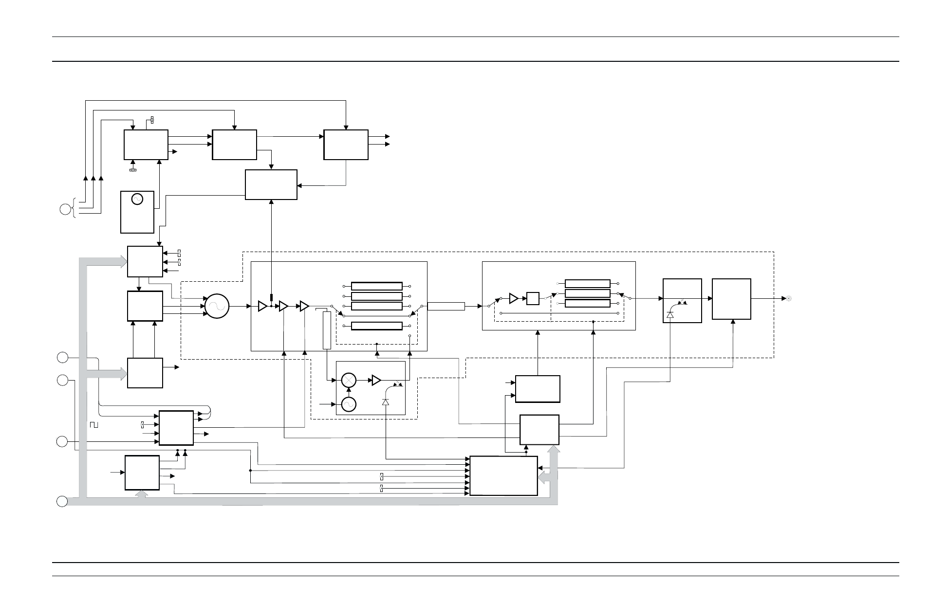
Figure 2-1. Block Diagram of a Typical 682XXB/683XXB
Synthesized Signal Generator (Sheet 2 of 2)
