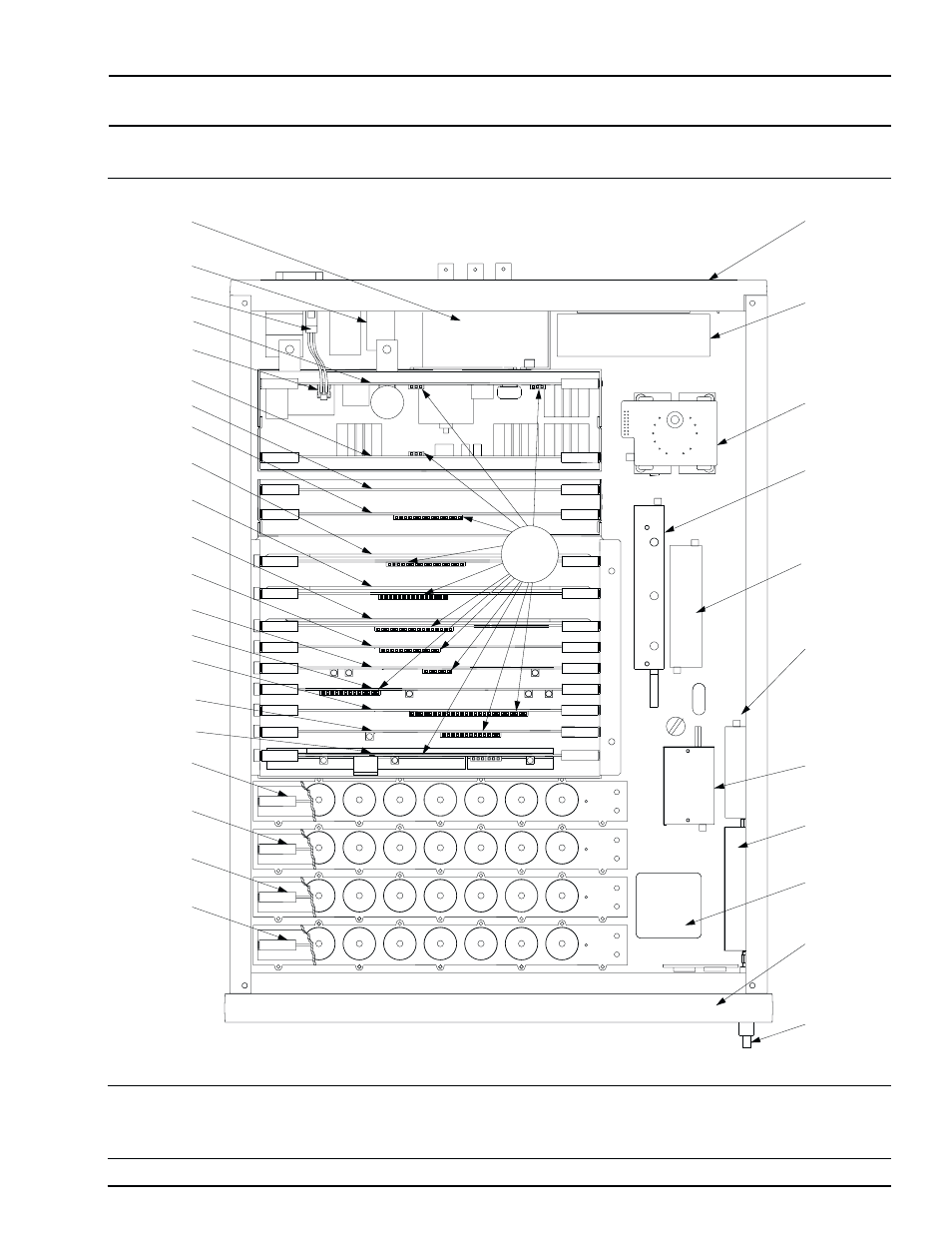
Assembly and component locator diagram, 6-9, Figure 6-3. assembly and component locator diagram – Anritsu 682XXB User Manual
Page 229

682XXB/683XXB MM
6-9
REMOVAL AND
PCB AND COMPONENT
REPLACEMENT PROCEDURES
LOCATOR DIAGRAM
J1
J2
J3
J4
J5
J6
J7
J1
J2
J3
J4
J5
J6
J7
J1
J2
J3
J4
J5
J6
J7
J1
J2
J3
J4
J5
J6
J7
Test
Points
Rear Panel
A15
Regulator PCB
A3
A4
A5
A6
A7
A9
A8
A10
A11
A12
A13
A14
A15
A16
A17
A18
A19
A3 Reference
Loop PCB
A4 Coarse
Loop PCB
A5 Fine
Loop PCB
A6 Pulse
Generator PCB
A8 Function
Generator PCB
A7 YIG
Loop PCB
A9 PIN
Control PCB
A10 ALC PCB
A11 FM PCB
A12 Analog
Instruction PCB
A13 YIG
Driver PCB
A14 SDM/SQM
Driver PCB
A16 CPU
Interface PCB
A17 CPU PCB
A18 Power
Supply PCB
A19P2
A19 Power
Conditioner PCB
A21P2
A21 Line Filter/
Rectifier PCB
A21-1
BNC/AUX I/0
Connector PCB
Fan Assy.
2-20 GHz
YIG Oscillator
Switched
Filter Assy.
Down Converter
Directional
Coupler
20-40 GHz
SDM
Step
Attenuator
(Option 2)
10 MHz Hi-Stab
Crystal Oscillator
(Option 16)
Front Panel Assy.
(Containing
A1 & A2 PCB's)
RF Output
Connector
Figure 6-3.
Assembly and Component Locator Diagram
