Rainbow Electronics AT76C551 User Manual
Page 54
54
AT76C551
1612D–08/01
USB_DMA_FADD: DMA Target Endpoint Address
addr 5000020h
R/W
16 bits
• Bits 7..0 – FAD[7:0]: USB Target Endpoint FIFO Address
Note:
Default: 00h
This register is programmed with the address of the Endpoint FIFO Register of the USB block
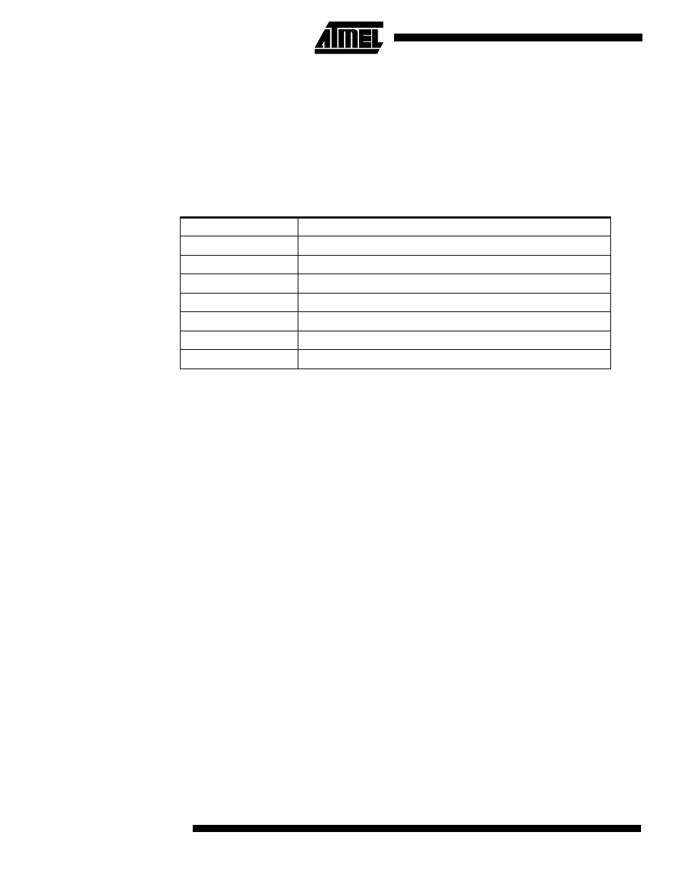
that the DMA operation is going to transfer bytes from/to. The addresses of the six endpoints
supported by the USB block are listed in Table 5.
USB_RDMA_LENR: Receive DMA Packet Length Transferred
addr 5000024h
R
8 bits
• Bits 7..0 URDL[7:0]: Receive DMA Transferred Length
Note:
Default: 00h
The contents of this register after the end of a DMA reflect the number of bytes that have been
transferred.
USB_RDMA_EN
addr 5000028h
R/W
8 bits
Bits 7..2 – Reserved
• Bit 1 – RDMAEN
Activates receive DMA (DMA for an OUT endpoint). This bit is reset after the completion of the
DMA.
• Bit 0 – Reserved
Note:
Default: 00h
USB_DMA_RADD: RAM Target Address for DMA Cycles
addr 5000040h
R/W
32 bits
• Bits 31..24 – Reserved
• Bits 23..0 – RAD[23:0]
Target address in SRAM for DMA transfers.
Note:
Default: 00h
USB_TDMA_LEN: Transmit DMA Packet Length Requested
addr 5000044h
R/W
16 bits
Table 5. DMA Target Endpoint Addresses
Address
Target
0xCF
FDR0 Function Endpoint0
0xCE
FDR1 Function Endpoint1
0xCD
FDR2 Function Endpoint2
0xCC
FDR3 Function Endpoint3
0xCB
FDR4 Function Endpoint4
0xCA
FDR5 Function Endpoint5
0xC9
FDR6 Function Endpoint6