Signal description – pin name order – Rainbow Electronics AT76C551 User Manual
Page 10
10
AT76C551
1612D–08/01
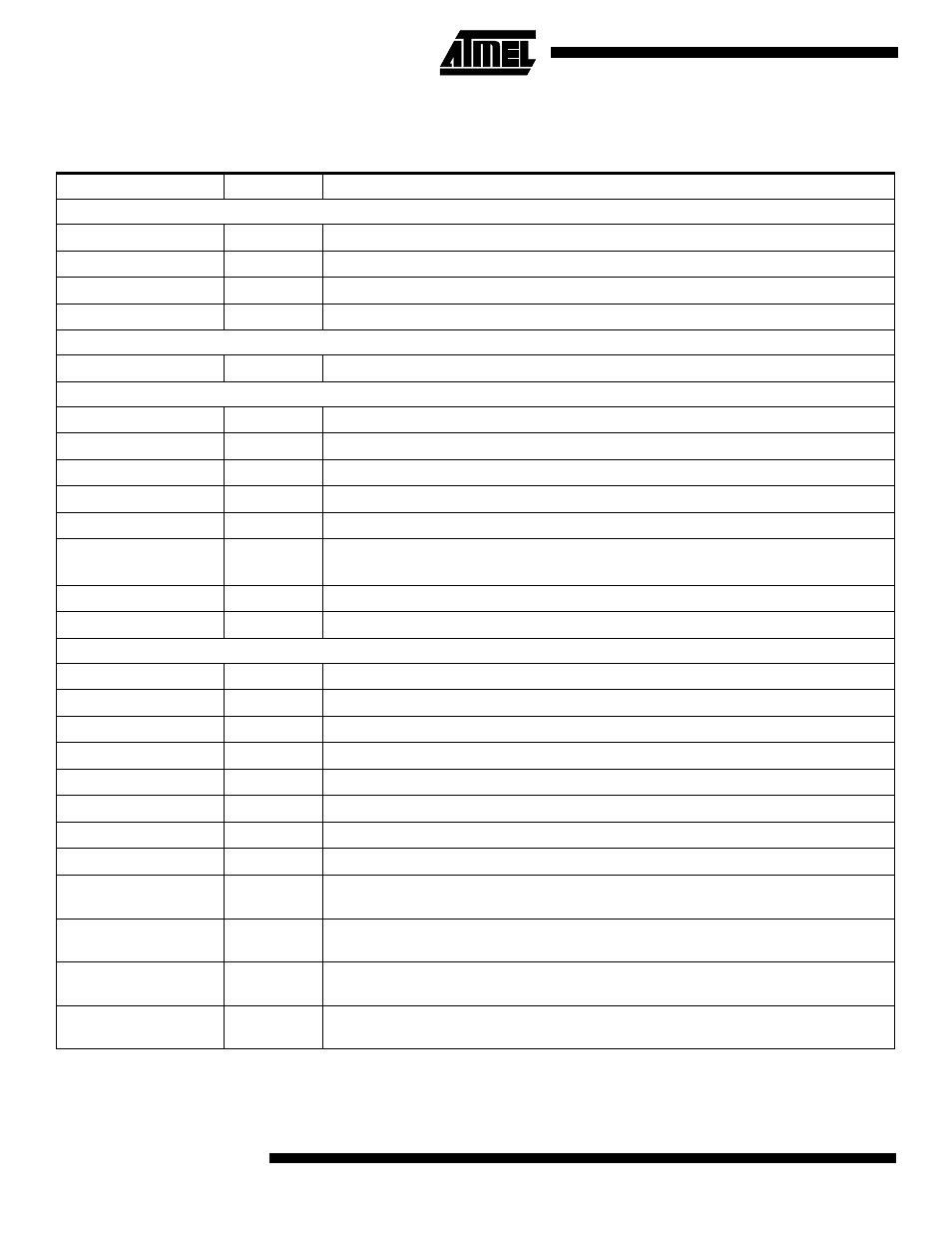
Signal Description – Pin Name Order
I = Input, O = Output, B = Bidirectional, Analog I = Analog Input, Analog O = Analog Output
Pin Name
Type
Description
Supply Pins
AGND
Power
Analog Ground
AVCC
Power
Analog Supply
GND
Power
Digital Ground
VCC
Power
Digital Supply
Global Pin
PC_RESET
I
Global Reset pin
Oscillator Pins
XTAL1
I
Crystal oscillator input
XATL2
O
Crystal oscillator output
EXT_13_MHZ
I
13 MHz input clock
EXT_13_MHZ_OUT
O
13 MHz output clock
EXT_OSC
I
External oscillator input
CLK_MODE1,
CLK_MODE0
I
Clock Frequency Configuration
OSC_MODE
I
Internal/Extenal Clock Selector
LFT
PLL Filter
PLL loop filter pin
Memory Interface Pins
CSFL16
O
Chip select when 16-bit Flash is used
CSSR
O
Chip select for low byte 8-bit SRAM
CSFL
O
Chip select for low byte Flash
CSSRH
O
Chip select for high byte SRAM
CSFLH
O
Chip select for high byte Flash
NWRITE
O
Memory write
NREAD
O
Memory read
NWORD
I
Selects between 8 and 16 memory access
MEM_ADDR [18:0]
O
Memory Address Bus – Signals MEM_ADDR [18:0] are address-bus output lines of Flash
and SRAM.
MEM_DATA [7:0]
B
Memory Data Bus – Signals MEM_DATA [7:0] are the bi-directional data bus lines for the
SRAM and Flash memory.
MEM_DATAH [7:0]
B
Memory Data Bus – Signals MEM_DATAH [7:0] are the bi-directional data bus lines for the
SRAM and Flash memory. These lines are used during 16-bit memory configuration.
P_OR_UN
I
Selects whether PCMCIA or USB will have direct access to the memories. When “1”
PCMCIA has direct access while when “0” USB has access