Internal architecture, Arm core, Memory interface – Rainbow Electronics AT76C551 User Manual
Page 17
17
AT76C551
1612D–08/01
Internal
Architecture
The AT76C551 chip is based on the ARM7TDMI processor. All modules are connected to the
processor through a 32-bit bus including 32 KB internal SRAM. The processor operates at 24
MHz while low speed operation of the ARM
®
processor and power-down of virtually all inter-
faces is possible.
ARM Core
The controller contains the ARM7TDMI (ARM7) core, a 32-bit RISC processor. The ARM7
core can execute all the functionally called for by the Bluetooth specification. ARM7 supports
two alternative instruction sets:
1.
Powerful 32-bit code can be executed by the processor in ARM
®
operating mode.
2.
Thumb
®
, which stores a subset of 32-bit instructions as compressed 16-bit instructions
and decompresses them back to 32 bits upon execution.
Utilization of Thumb mode will exploit full processor power with limited external memory
resources.
Note:
ARM7TDMI operating mode can be changed at run time with negligible overhead.
Memory Interface
The memory interface interfaces the ARM processor to the 32K internal SRAM and external
Flash and SRAM memory that accompanies a complete design. Flash memory contains the
Bluetooth and Host Interface firmware and the Card Information Structure (CIS) used by the
host PCMCIA subsystem. Either 8-bit or 16-bit Flash memories and 8-bit SRAMs can be used.
The internal 32K SRAM memory accommodates ARM core stack, firmware status variables,
structures supporting host/firmware interface and network data buffers. When the host driver
software passes network data through the PCMCIA interface unit, the data can be automati-
cally routed to either internal or external memories.
Note:
Firmware performance is optimized by permanently storing it in a slow Flash. Upon initialization
it is loaded onto faster SRAM to fetch the instructions.
External memory can be either 8-bit or 16-bit wide. External memory width is configured via
the NWORD pin. When 8-bit memory is used, up to 512 kilobytes of SRAM and Flash memory
is supported. When 16-bit memory is used, up to 1 megabyte of SRAM and Flash memory is
supported.
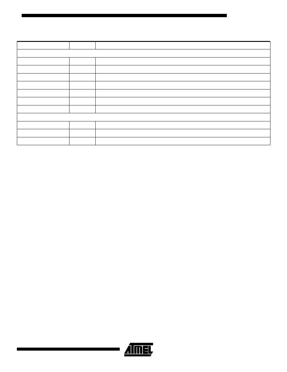
JTAG Pins
DB_DATA
O
Debug data port
DB_CLK
O
Debug clock port
NTRST
I
JTAG reset input
TCK
I
JATG clock
TDI
I
JTAG data input
TDO
I
JTAG data output
TMS
I
JTAG master select input
TEST Pins
TEST_CTRL
I
For production test
TEST_ECK
I
For production test
PLL_TEST_PIN
I
For production test
Functional Description – Pin Name Order (Continued)
Name
Type
Description