1 rtc registers and ram, 1 rtc registers and ram -14, Rtc (standard) ram bank -14 – Intel 460GX User Manual
Page 284
PCI/LPC Bridge Description
15-14
Intel® 460GX Chipset Software Developer’s Manual
The time and calendar data should match the data mode (BCD or binary) and hour mode (12 or 24
hour) as selected in register B. It is up to the programmer to make sure that data stored in these
locations is within the reasonable values ranges and represents a possible date and time. The
exception to these ranges is to store a value of C0 - FF in the Alarm bytes to indicate a don’t care
situation. All Alarm conditions must match to trigger an Alarm Flag, which could trigger an Alarm
Interrupt if enabled. The UIP bit should be read as 0 before each access to these registers. The SET
bit of register B should be one while programming these locations to avoid clashes with an update
cycle. Access to time and date information is done through the RAM locations. If a RAM read
from the ten time and date bytes is attempted during an update cycle, the value read will not
necessarily represent the true contents of those locations. Any RAM writes under the same
conditions will be ignored.
15.5.1
RTC Registers and RAM
The RTC internal registers and RAM are organized as two banks of 128 bytes each, called the
standard and extended banks. The first 14 bytes of the standard bank contain the RTC time and date
information along with four registers, A - D, that are used for configuration of the RTC. The
extended bank contains a full 128 bytes of battery backed SRAM, and will be accessible even when
the RTC module is disabled (via the RTC configuration register).
All data movement between the host CPU and the real-time clock is done through registers mapped
to the I/O space at locations 70-73h.
I/O locations 70h and 71h are the standard RAM location for the real-time clock. I/O locations 72h
and 73h are the extended RAM, and may be disabled. When disabled, 72h and 73h become aliases
for 70h and 71h respectively. The addressing is done by a indexing scheme: 70h (72h) is written
with the index, and 71h (73h) is written with data or read for data. This scheme is shown in
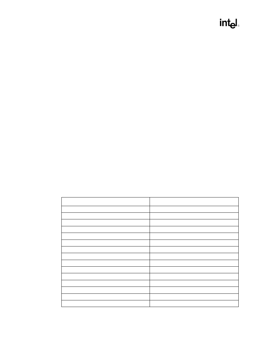
Table 15-2. RTC (Standard) RAM Bank
Index Address
Name
00h
Seconds
01h
Seconds Alarm
02h
Minutes
03h
Minutes Alarm
04h
Hours
05h
Hours Alarm
06h
Day of Week
07h
Date of Month
08h
Month
09h
Year
0Ah
Register A
0Bh
Register B
0Ch
Register C
0Dh
Register D
0Eh - 7Fh
114 Bytes of User RAM