5 ultra dma configuration, Configuration offset 48h) -2, Configuration offsets 4a-4bh) -2 – Intel 460GX User Manual
Page 172
IFB Usage Considerations
10-2
Intel® 460GX Chipset Software Developer’s Manual
into the system firmware by the vendor. This reporting will make these register locations safe and
the OS will not use these locations randomly if a PNP conflicting device is relocatable in those I/O
or memory locations. These locations also got to be reported to the OS whenever the OEM sends
the systems for their WHQL suite test.
10.5
Ultra DMA Configuration
The following registers are programmed in systems that contain devices that implement the Ultra
DMA Protocol. These registers allow Ultra DMA to be used when PCI Bus Master IDE operation
is initiated by the device driver.
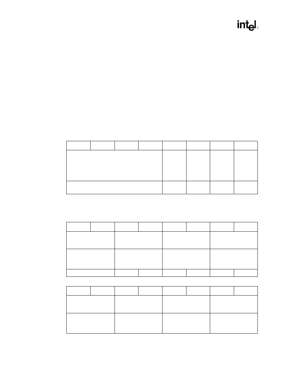
10.5.1
UDMAC–Ultra DMA Control Register (IFB Function 1 PCI
Configuration Offset 48h)
10.5.2
UDMATIM–Ultra DMA Timing Register (IFB Function 1 PCI
Configuration Offsets 4A-4Bh)
7
6
5
4
3
2
1
0
Reserved
Secondary
Drive 1
Ultra DMA
Mode
Enable
(SSDE1)
Secondary
Drive 0
Ultra DMA
Mode
Enable
(SSDE0)
Primary
Drive 1
Ultra DMA
Mode
Enable
(PSDE1)
Primary
Drive 0
Ultra DMA
Mode
Enable
(PSDE0)
0: Disabled
1: Enabled
0: Disabled
1: Enabled
0: Disabled
1: Enabled
0: Disabled
1: Enabled
15
14
13
12
11
10
9
8
Reserved
Secondary Drive 1
Ultra DMA Cycle Time
(SCT1)
Reserved
Secondary Drive 0
Ultra DMA Cycle Time
(SCT1)
00: CT=4 clks, RP=6 clks
01: CT=3 clks, RP=5 clks
10: CT=2 clks, RP=4 clks
11: Reserved
00: CT=4 clks, RP=6 clks
01: CT=3 clks, RP=5 clks
10: CT=2 clks, RP=4 clks
11: Reserved
7
6
5
4
3
2
1
0
Reserved
Primary Drive 1
Ultra DMA Cycle Time
(PCT1)
Reserved
Primary Drive 0
Ultra DMA Cycle Time
(PCT1)
00: CT=4 clks, RP=6 clks
01: CT=3 clks, RP=5 clks
10: CT=2 clks, RP=4 clks
11: Reserved
00: CT=4 clks, RP=6 clks
01: CT=3 clks, RP=5 clks
10: CT=2 clks, RP=4 clks
11: Reserved