2 access restrictions, 1 partitioning, Access restrictions -2 2.2.1 – Intel 460GX User Manual
Page 22: Partitioning -2, Device mapping on bus cbn -2
Register Descriptions
2-2
Intel® 460GX Chipset Software Developer’s Manual
to a PCI bus. Reads result in data being returned by the xXB through the SAC to the system
bus.
•
Otherwise, the access is forwarded to the xXB to be placed on the PCI bus (or AGP bus) as a
Configuration Read or Configuration Write cycle. Reads will result in data being returned
through the xXB and SAC back to the system bus, just as in normal Outbound Read
operations.
2.2
Access Restrictions
The 460GX chipset supports PCI configuration space access using the mechanism denoted as
Configuration Mechanism #1 in the PCI specification.
The 460GX chipset internal registers (both I/O Mapped and Configuration registers) are accessible
by the Host CPU. The registers can be accessed as Byte, Word (16-bit), or Dword (32-bit)
quantities, with the exception of CONFIG_ADDRESS which can only be accessed as a Dword. All
multi-byte numeric fields use “little-endian” ordering (i.e. lower addresses contain the least
significant parts of the field).
2.2.1
Partitioning
Each SAC, SDC, MAC, PXB, WXB, GXB, each AGP bus below an GXB, and each PCI bus below
an PXB or WXB, has an independent configuration space. None of the registers are shared between
the spaces; that is, the SAC, and each PCI bus in the PXB, have separate control and status
registers.
Configuration registers are accessed using an “address” comprised of the PCI Bus Number, the
Device Number within the bus, and the Register Number within the Device.
Accesses to devices on Bus #0 and Bus #(CBN) are serviced by the 460GX chipset depending on
their device number. Device 10h on Bus #0 is mapped to the SAC; it contains the programmable
Chipset Bus Number. All other chipset devices reside on bus CBN.
The DEVNPRES register is used to determine which chipset devices are present; see
for
mapping information.
Configuration registers located in the SDC are accessed over the private data bus. The SAC
translates CF8/CFC accesses to SDC registers into configuration commands over the PDB.
Configuration registers located on the memory boards are accessed over the I2C port. The SAC
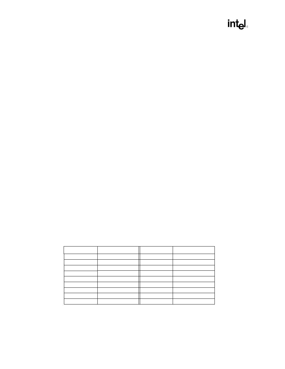
Table 2-1. Device Mapping on Bus CBN
No.
Device
No.
Device
00h
SAC
10h
Expander 0, Bus a
a
a. This is the compatibility bus (where the boot vector is always directed).
01h
SAC
11h
Expander 0, Bus b
02h
reserved
12h
Expander 1, Bus a
03h
reserved
13h
Expander 1, Bus b
04h
SDC
14h
Expander 2, Bus a
05h
Memory Card A
15h
Expander 2, Bus b
06h
Memory Card B
16h
Expander 3, Bus a
07h
reserved
17h
Expander 3, Bus b
08h-0Fh
reserved
18h-1Fh
reserved