3 ide controller i/o space registers, 1 bmicx–bus master ide command register (i/o), Ultra dma/33 timing mode settings -9 – Intel 460GX User Manual
Page 241

Intel® 460GX Chipset Software Developer’s Manual
12-9
IDE Configuration
NOTES:
1.
assumes that if the attached slave drive is Mode 0 or not present, the SITRE bit is ‘0’.
2.
assumes that 25 MHz is not supported as a target PCI system speed. If the DMA Timing Enable
Only (DTE) bit has been enabled for that drive, this resultant cycle time applies to data transfers performed
with DMA only.
12.3
IDE Controller I/O Space Registers
The PCI IDE Function uses 16 bytes of I/O space, allocated via the BMIBA register. All bus master
IDE I/O space registers can be accessed as byte, word, or DWord quantities. The description of the
16 bytes of I/O registers follows.
12.3.1
BMICx–Bus Master IDE Command Register (I/O)
Address Offset:
Primary Channel–Base + 00h; Secondary Channel–Base + 08h
Default Value:
00h
Attribute:
Read/Write
This register enables/disables bus master capability for the IDE Function and provides direction
control for the IDE DMA transfers. This register also provides bits that software uses to indicate
DMA capability of the IDE device.
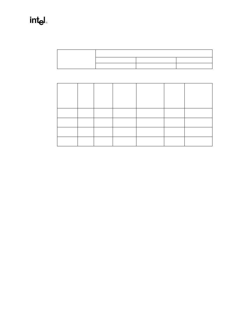
Table 12-2. Ultra DMA/33 Timing Mode Settings
Cycle Time Bit Settings
Ultra DMA/33 Timing Modes
Mode 0 (120 ns)
Mode 1 (90 ns)
Mode 2 (60 ns)
00
01
10
Table 12-3. DMA/PIO Timing Values Based on IFB Cable Mode and System Speed
IFB Drive
Mode
IORDY
Sample
Point
(ISP)
Recovery
Time
(RCT)
IDETIM [15:8]
Drive 0
(Master)
If Slave
Attached
IDETIM [15:8]
Drive 0 (Master)
If no Slave
Attached or
Slave is
Mode 0
1
SIDETIM
Pri [3:0]
Sec [7:4]
Drive 1
(Slave)
Resultant
Cycle Time
Base Operating
Frequency and
Cycle Time
2
PIO0/
Compatible
6 clocks
(Default)
1 clocks
(Default)
C0h
80h
0
30 MHz: 660ns
33 MHz: 600ns
PIO2/SW2
4 clocks
4 clocks
D0h
90h
4
30 MHz: 256ns
33 MHz: 240ns
PIO3/MW1
3 clocks
3 clocks
E1h
A1h
9
30 MHz: 198ns
33 MHz: 180ns
PIO4/MW2
3 clocks
1 clock
E3h
A3h
B
30 MHz: 132ns
33 MHz: 120ns
