3 block diagram, 4 processor, 3 block diagram 4.4 processor – Artesyn MVME6100 Single Board Computer Installation and Use (June 2014) User Manual
Page 65: Figure 4-1, Mvme6100 block diagram, Functional description
Functional Description
MVME6100 Single Board Computer Installation and Use (6806800D58H)
65
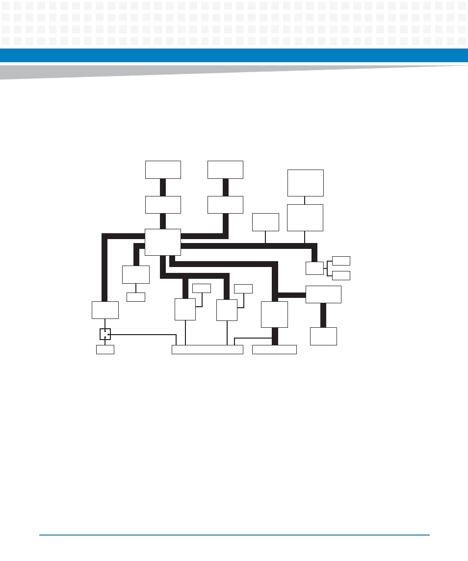
4.3
Block Diagram
shows a block diagram of the overall board architecture.
4.4
Processor
The MVME6100 supports the MPC7457 with adjustable core voltage supply. The maximum
external processor bus speed is 133 MHz. The processor core frequency runs at 1.267 GHz or
the highest speed MPC7457 can support, which is determined by the processor core voltage,
the external speed, and the internal VCO frequency. MPX bus protocols are supported on the
board. The MPC7457 has integrated L1 and L2 caches (as the factory build configuration) and
supports an L3 cache interface with on-chip tags to support up to 2MB of off-chip cache. +2.5V
signal levels are used on the processor bus.
Figure 4-1
MVME6100 Block Diagram
64-bit/33/66/100 MHz PCI-X
L3 Cache
2MB
MPC7457
1.267 GHz
211 MHz SDR
133 MHz
Processor Bus
133 MHz
Memory Bus
RTC
NVRAM
VME
TSI148
Soldered
Flash
Bank A
64MB
64-bit/133 MHz PCI-X
DDR RAM
512MB-1GB
DDR RAM
512MB-1GB
Rows D&Z
46-pins
Gigabit
Ethernet
RJ-45
Jumper
Selectable
Soldered
Flash
Bank B
64MB
32/64-bit,
33/66 MHz PC
4250 0604
Discovery II
Host
Bridge
Device Bus
Gigabit
Ethernet
RJ-45
IPMC
Slot 2
FP I/O
P2
P1
PMC Span
Connector
P-P Br
idge
Serial
RJ-45
header
Rows A&C
64-pins
PMC
Slot 1
FP I/O