Address and command datapath –9, Address and command datapath – Altera External Memory PHY Interface User Manual
Page 77
Chapter 4: Support for Arria GX, HardCopy II, Stratix II, and Stratix II GX Devices
4–9
DDR2/DDR SDRAM
© January 2010
Altera Corporation
External Memory PHY Interface (ALTMEMPHY) (nonAFI) Megafunction User Guide
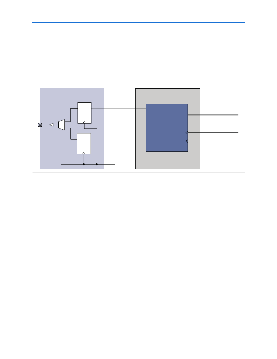
The memory controller interface outputs 4n-bit wide data (ctl_wdata[4n]) at half-
rate frequency.
shows that the HDR write data (ctl_wdata[4n]) is
clocked by the half-rate clock phy_clk_1x and is converted into SDR which is
represented by wdp_wdata_h and wdp_wdata_l and clocked by the full-rate clock
write_clk_2x
.
The DQ IOEs convert 2-n SDR bits to n-DDR bits.
Address and Command Datapath
The address and command datapath is responsible for taking the address and
command outputs from the controller and converting them from half-rate clock to
full-rate clock. Two types of addressing are possible:
■
1T (full rate)—The duration of the address and command is a single memory clock
cycle (mem_clk_2x,
). This applies to all address and command signals
in full-rate designs or mem_cs_n, mem_cke, and mem_odt signals in half-rate
designs.
■
2T (half rate)—The duration of the address and command is two memory clock
cycles. For half-rate designs, the ALTMEMPHY megafunction supports only a
burst size of four, which means the burst size on the local interface is always set to
1
. The size of the data is 4n-bits wide on the local side and is n-bits wide on the
memory side. To transfer all the 4n-bits at the double data rate, two memory-clock
cycles are required. The new address and command can be issued to memory
every two clock cycles. This scheme applies to all address and command signals,
except for mem_cs_n, mem_cke, and mem_odt signals in half-rate mode.
f
Refer to
in
to see the frequency relationship of
mem_clk_2x
with the rest of the clocks.
shows a 1T chip select signal (mem_cs_n), which is active low, and
disables the command in the memory device. All commands are masked when the
chip-select signal is inactive. The mem_cs_n signal is considered part of the command
code.
Figure 4–4. DDR2/DDR SDRAM Write Datapath in Arria GX, HardCopy II, Stratix II, and Stratix II GX Devices
Write Datapath
Stratix II IOE
wdp_wdata_l
phy_clk_1x (ctl_clk)
D
Q
D
Q
OE
DQ[n]
write_clk_2x
ctl_wdata[4n]
write_clk_2x
Data
Multiplexing
wdp_wdata_h