Altera External Memory PHY Interface User Manual
Page 18
3–2
Chapter 3: Functional Description—ALTMEMPHY (nonAFI)
QDR II+/QDR II SRAM Calibration Process
External Memory PHY Interface (ALTMEMPHY) (nonAFI) Megafunction User Guide
© January 2010
Altera Corporation
The clock CQ coming from the QDR II+/QDR II SRAM is delayed and is divided by
two to generate a half-rate clock (resync_clk_1x). Data is captured on the rising
edges of the shifted CQ and shifted CQn signals. There is one resync_clk_1x per
DQS group. QDR II+/QDR II SRAM devices can only have one DQS group per
device, which means that there is one resync_clk_1x signal associated with each
memory device. This signal clocks the registers doing the full-rate to half-rate
conversion. It also clocks the front side of the read datapath clock-crossing FIFO.
There is one FIFO per DQS group (or memory device).
The resync_clk_1x signal can be inverted or not inverted. You can transfer data in
the correct byte order with one of these options. The main objective of calibration is to
find out whether the resync_clk_1x signal requires inversion, which is done by
loading the shift register, see
(at most twice per QDR II+/QDR II SRAM
device). Each memory device is calibrated one after the other.
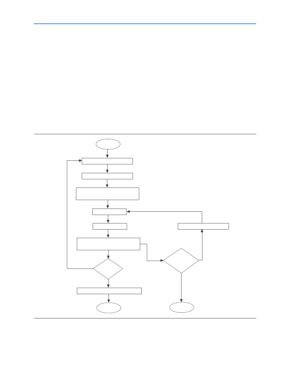
shows the QDR II+/QDR II SRAM calibration flowchart.
Figure 3–2. QDR II+/QDR II SRAM Calibration Flowchart
Calibration start
Write 0's pattern to address 3
Write 1's pattern to address 5
Setup resync_clk_1x phase associated with
DQS group being calibrated
Read 0's pattern
Read 1's pattern
Start latency counter and search for
0's followed by 1's pattern
All DQS groups
calibrated?
Align all DQS groups to worst case latency
Calibration
successful
Yes
No
Timed out for both
phases of
resync_clk_1x
Invert resync_clk_1x phase
No
Latency counter
timeout
Calibration
unsuccessful
Yes
If pattern found