Note 1) – Altera External Memory PHY Interface User Manual
Page 26
3–10
Chapter 3: Functional Description—ALTMEMPHY (nonAFI)
ALTMEMPHY Signals
External Memory PHY Interface (ALTMEMPHY) (nonAFI) Megafunction User Guide
© January 2010
Altera Corporation
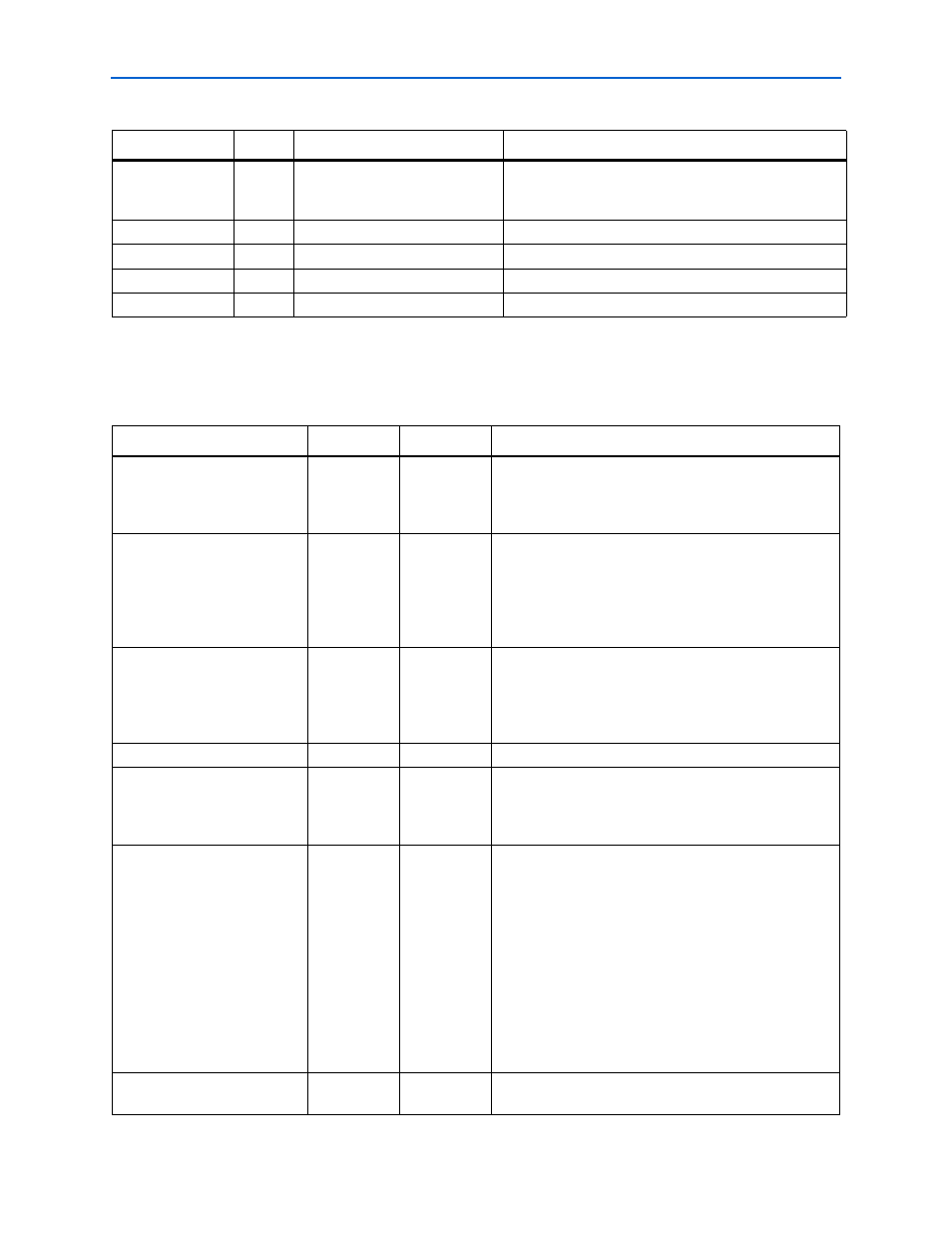
mem_dqsn
bidir
MEM_IF_DWIDTH /
MEM_IF_DQ_PER_DQS
The memory bidirectional data strobe bus. Not used in
Arria GX, HardCopy II, Stratix II, and Stratix II GX
designs.
mem_odt
output
MEM_IF_CS_WIDTH
The memory on-die termination control signal.
mem_ras_n
output
1
The memory row address strobe.
mem_reset_n
output
1
The memory-reset signal.
mem_we_n
output
1
The memory write-enable signal.
Notes to
(1) Connected to I/O pads.
(2) Output is for memory device, and input path is fed back to ALTMEMPHY megafunction for VT tracking.
Table 3–1. I/O Interface for DDR2 and DDR SDRAM—nonAFI
(Note 1)
(Part 2 of 2)
Signal Name
Type
Width
Description
Table 3–2. Clock and Reset Signals for DDR2/DDR SDRAM—nonAFI
(Part 1 of 2)
Signal Name
Type
Width
Description
global_reset_n
input
1
The asynchronous reset input to the controller. All other
reset signals are derived from resynchronized versions of
this. This signal holds the complete ALTMEMPHY
megafunction, including the PLL, in reset while low.
soft_reset_n
input
1
The asynchronous reset input to reset controller, for
SOPC Builder use, or to be controlled by other system
reset logic. This signal causes a complete reset of the
PHY, but not the PLL in the PHY. In Arria GX, Stratix II,
and Stratix II GX devices, this signal also resets the PLL
reconfiguration block on a falling-edge detection.
phy_clk
output
1
The ALTMEMPHY megafunction half-rate clock provided
to the user. All user inputs and outputs to the
ALTMEMPHY megafunction are synchronous to this clock
in half-rate designs. However, this clock is not used in
full-rate designs.
pll_ref_clk
input
1
The reference clock input to PLL.
reset_phy_clk_n
output
1
Asynchronous reset, that is de-asserted synchronously
with respect to the associated phy_clock clock
domain. Use this to reset any additional user logic on that
clock domain.
reset_request_n
output
1
Directly connected to the locked output of the PLL and is
intended for optional use either by automated tools such
as SOPC Builder or could be manually ANDed with any
other system-level signals and combined with any edge
detect logic as required and then fed back to the
global_reset_n
input.
Reset request output that indicates when the PLL outputs
are not locked. Use this as a reset request input to any
system-level reset controller you may have. This signal is
always low while the PLL is locking (but not locked), and
so any reset logic using it is advised to detect a reset
request on a falling-edge rather than by level detection.
aux_half_rate_clk
output
1
A copy of the phy_clk_1x signal that you can use in
other parts of your design, same as phy_clk port.