Altera External Memory PHY Interface User Manual
Page 73
Chapter 4: Support for Arria GX, HardCopy II, Stratix II, and Stratix II GX Devices
4–5
DDR2/DDR SDRAM
© January 2010
Altera Corporation
External Memory PHY Interface (ALTMEMPHY) (nonAFI) Megafunction User Guide
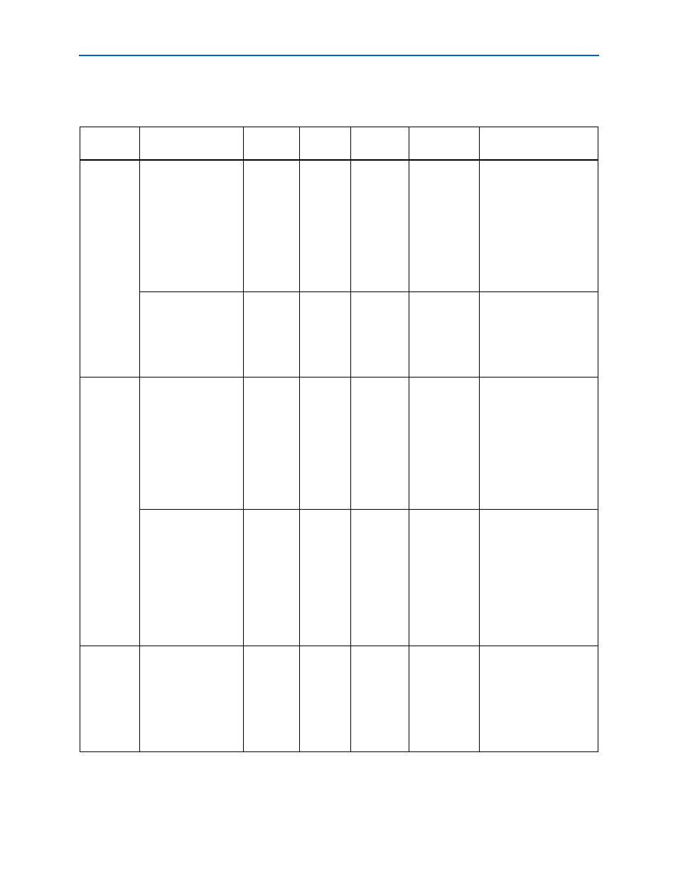
shows the clock outputs that Arria GX, HardCopy II, Stratix II and
Stratix II GX devices use.
Table 4–1. DDR2/DDR SDRAM Clocking in Arria GX, HardCopy II, Stratix II, and Stratix II GX Devices (Part 1 of 2)
Design
Rate
Clock Name
Postscale
Counter
Phase
(Degrees)
Clock Rate
Clock
Network Type
Notes
Half-rate
phy_clk_1x
and
aux_half_rate_
clk
C0
0
Half-Rate
Global
The only clock that is
made available on the user
interface of the
ALTMEMPHY
megafunction. This clock
also feeds into a divider
circuit to provide the PLL
scan_clk
signal (for
reconfiguration) that must
be lower than 100 MHz.
mem_clk_2x
and
aux_full_
rate_clk
C1
0
Full-Rate
Global
This clock is for clocking
DQS and as a reference
clock for the memory
devices.
Full rate
aux_half_rate_
clk
C0
0
Half-Rate
Global
The only clock that is
made available on the user
interface of the
ALTMEMPHY
megafunction. This clock
also feeds into a divider
circuit to provide the PLL
scan_clk
signal (for
reconfiguration) that must
be lower than 100 MHz.
and
mem_clk_2x
and
aux_full_
rate_clk
C1
0
Full-Rate
Global
This clock is for clocking
DQS and as a reference
clock for the memory
devices.
Half-rate
and full rate
write_clk_2x
C2
–90
Full-Rate
Global
This clock is for clocking
the data out of the DDR
I/O (DDIO) pins in
advance of the DQS strobe
(or equivalent). As a
result, its phase leads that
of the mem_clk_2x by
90°.