Ddr2 sdram initialization timing –7, Ddr2 sdram initialization timing” on, Ddr2 sdram initialization timing – Altera External Memory PHY Interface User Manual
Page 23: Nop (for 200 µs, programmable), Elmr, register 2, Elmr, register 3, Elmr, register 1, Time to make simulation easier
Chapter 3: Functional Description—ALTMEMPHY (nonAFI)
3–7
Initialization Timing
© January 2010
Altera Corporation
External Memory PHY Interface (ALTMEMPHY) (nonAFI) Megafunction User Guide
DDR2 SDRAM Initialization Timing
The DDR2 SDRAM high-performance controller initializes the memory devices by
issuing the following command sequence:
■
NOP (for 200 µs, programmable)
■
PCH
■
ELMR, register 2
■
ELMR, register 3
■
ELMR, register 1
■
LMR
■
PCH
■
ARF
■
ARF
■
LMR
■
ELMR, register 1
■
ELMR, register 1
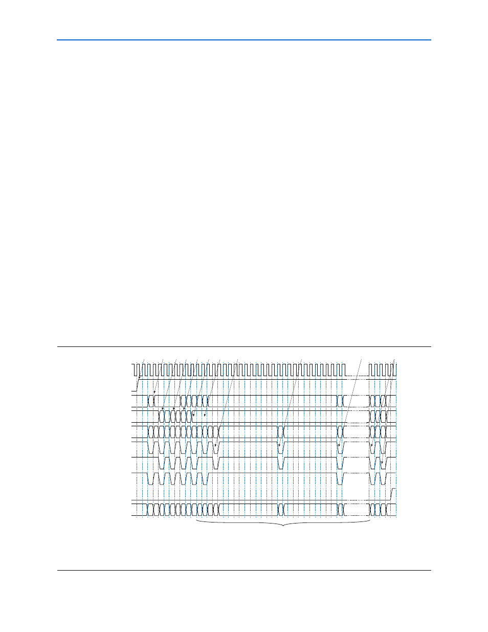
shows a typical DDR2 SDRAM initialization timing sequence, which is
described below. The length of time between the reset and the clock enable signal
going high should be 200 µs. The value that you choose for the Memory initialization
time at power up (tINIt)
setting in the MegaWizard interface is only used for
hardware that you generate. The controller simulation model is created with a much
shorter t
INIT
time to make simulation easier.
Figure 3–5. DDR2 SDRAM Device Initialization Timing
Note to
(1) local_init_done only goes high when calibration has completed.
Key:
P = PCH
L = LMR
A = ARF
clk
ddr_cke
ddr_a
ddr_ba
ddr_cs_n
ddr_ras_n
ddr_cas_n
ddr_we_n
local_init_done
DDR Command
2 0 3 0 1 0
0
1 0 1 1
1
0
0
0
0
0
0
0
P
L
L
L
L
P
A
A
L
N
L
L
L
200 clock cycles
[1]
[2]
[3]
[3]
[4]
[7]
[6]
[5]
[7]
[8]
[9]