Ctl_mem_addr_h, Ctl_mem_cas_n_h – Altera External Memory PHY Interface User Manual
Page 61
Chapter 3: Functional Description—ALTMEMPHY (nonAFI)
3–45
Design Considerations
© January 2010
Altera Corporation
External Memory PHY Interface (ALTMEMPHY) (nonAFI) Megafunction User Guide
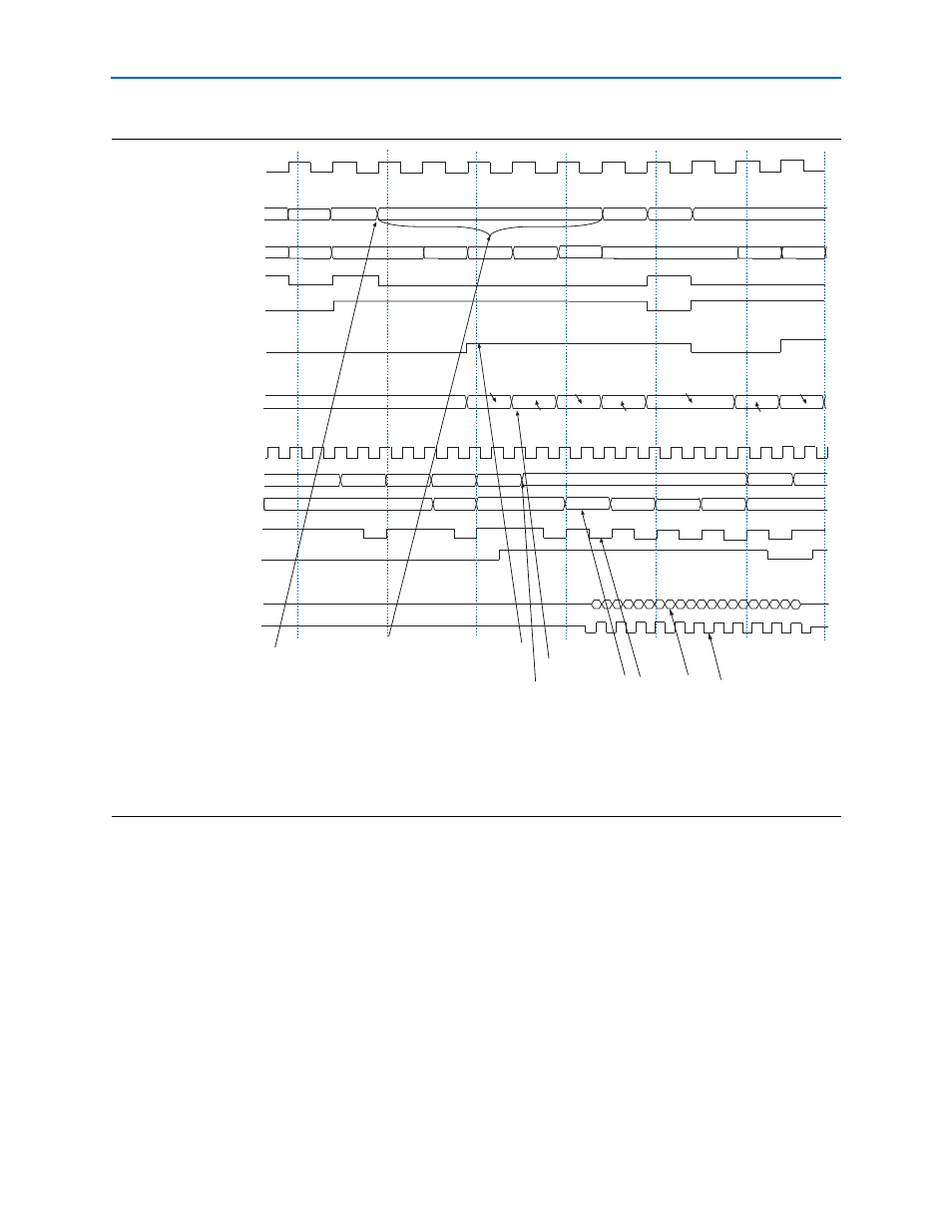
shows the sequence of operations that happen during the write
transactions. The write operation is explained step-by-step below. All the inputs to the
ALTMEMPHY megafunction from the controller should be generated using
phy_clk
.
1
The signals under the PHY command input label are the signals from the controller to
the ALTMEMPHY megafunction and the signals under the PHY command output
label are the signals coming out of the ALTMEMPHY megafunction and input to the
memory device.
Some of the address and command signals generated by the controller are:
■
ctl_mem_addr_h
■
ctl_mem_cas_n_h
Figure 3–13. Write Commands and Write Data (Half-Rate Controller)
Notes to
:
(1) The DDR command shows the command comprised of the command signals (ctl_mem_ras_n_h, ctl_mem_cas_n_h, and
ctl_mem_we_n_h)
seen at the ALTMEMPHY input. There can be more than one clock cycle of NOP between ACT to RD depending on the value
of t
RCD
parameter of your memory device.
(2) The DDR command shows the command comprised of the command signals (mem_ras_n_h, mem_cas_n_h, and mem_we_n_h) seen
at the memory interface.
DDR Command
(Note 1)
phy_clk
ctl_mem_addr_h
ctl_mem_cs_n_h
ctl_mem_odt_h
mem_addr
mem_cs_n
mem_odt
mem_dq
ctl_mem_wdata_valid
ctl_mem_wdata
0000
0003
0000
0004
0008
000C
0010
0000
mem_dqs[1]
PHY Command Input
PHY Write Data Input
PHY Command Output
PHY Write Data Output
1
2
3
3
4
6
7
DDR Command
(Note 2)
NOP
PCH
NOP
ACT
NOP
WR
ACT
NOP
5
5
mem_clk
ACT
ACT
NOP
NOP
WR
WR
0003
0000
0004
0008
000C
0010
0000
0004
0008
cdb042d1cc72ad13
877d84bf...
13a1563...
26e92ac...
4ccf5491...
9883a83fb8e6045a
2d1b4d7...
5a369af...