Figure 3–14 – Altera External Memory PHY Interface User Manual
Page 64
3–48
Chapter 3: Functional Description—ALTMEMPHY (nonAFI)
Design Considerations
External Memory PHY Interface (ALTMEMPHY) (nonAFI) Megafunction User Guide
© January 2010
Altera Corporation
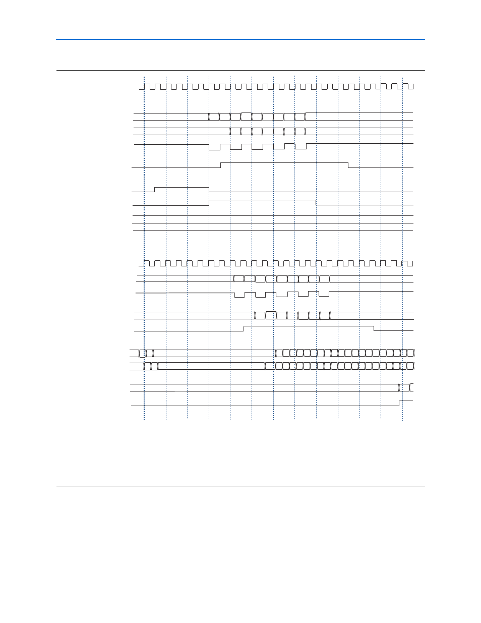
Figure 3–14. Read Commands and Read Data (Full-Rate Controller)
Notes to
:
(1) The DDR command shows the command comprised of the command signals (ctl_mem_ras_n_h, ctl_mem_cas_n_h, and
ctl_mem_we_n_h)
seen at the ALTMEMPHY input. There can be more than one clock cycle of NOP between ACT to RD depending on the value
of t
RCD
parameter of your memory device.
(2) The DDR command shows the command comprised of the command signals (mem_ras_n_h, mem_cas_n_h, and mem_we_n_h) seen
at the memory interface. There can be more than one clock cycle of NOP between ACT to RD depending on the value of the t
RCD
parameter of your
memory device.
phy_clk
ctl_mem_cs_n_h
ctl_mem_addr_h
ctl_mem_odt_h
DDR command (
1)
mem_clk
mem_addr
mem_odt
mem_dqs
mem_dq
ctl_mem_rdata
local_read_req
ctl_mem_rdata_valid
DDR command (
2)
mem_cs_n
PHY Command Input
PHY Read Data Input
PHY Command Output
Memory Interface
PHY Read Data Output
NOP
RD
NOP
ctl_doing_rd
count_wr
local_ready
RD
NOP RD
NOP RD
NOP RD
NOP
0000
0004 0000 0008 0000 000c 0000 0010 0000
0000
NOP
RD
NOP RD
NOP RD
NOP RD
NOP
0004
0000
0000 0008 0000 000c 0000
NOP RD
0010 0000
e... 8... 000000
1... 4... 3...
7... 0... f... 0...
0... c... 0...
1... 3... 2... 7...
e... 8...
0000
0...
0000 1... 0... 1...
1... 0... 1... 0...
0... 1... 0...
0... 1... 0... 1...
1... 0...
808bdae4ec55833a
473d 8