Table 2–3 – Altera External Memory PHY Interface User Manual
Page 12
2–6
Chapter 2: Parameter Settings
External Memory PHY Interface (ALTMEMPHY) (nonAFI) Megafunction User Guide
© January 2010
Altera Corporation
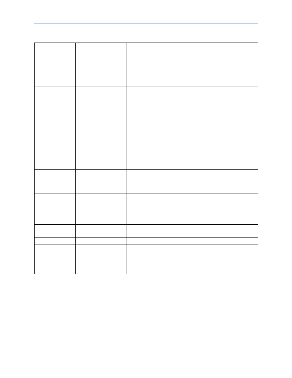
Table 2–3. QDR II+/QDR II SRAM Attribute Settings
Parameter Name
Range
Units
Description
De-rate ×18 timing
for emulation ×36
mode
Enabled or Disabled
—
Allows the ALTMEMPHY megafunction to derate the timing
calculation when creating ×36 QDR II+/QDR II SRAM
interfaces by using two ×18 DQS/DQ groups. For more
information on ×36 emulation, refer to
x36 QDR II+/QDR II SRAM ALTMEMPHY Variation” on
page 2–7
Output clock pairs
from FPGA
1–16
pairs
Selects the number of differential clock pairs driven from the
FPGA to the memory. More clock pairs reduce the loading of
each output when interfacing with multiple memory devices.
Memory clock pins use the signal splitter feature in Stratix III
and Stratix IV devices for differential signaling.
Memory depth
expansion
1–2
chips
Picks the number of chip selects of memory supported. This
option is for memory depth expansion.
Memory interface
D/Q data bits
8–288
bits
Defines the width of external memory read and write data bus.
Multiply the number of devices with the number of DQ pins
per device when you create width-expanded memory
interfaces. Even though the GUI allows you to choose 288-bit
DQ width, the interface data width is limited by the number of
pins on the device. For best performance, have the whole
interface on one side of the device.
Memory vendor
Others
—
Displays the name of the memory vendor for all supported
memory standards.The ALTMEMPHY megafunction only has
generic QDR II+/QDR II SRAM data sheet information listed
under vendor as Other.
Maximum memory
frequency
See the memory device
data sheet
MHz
Defines the maximum frequency supported by the memory.
Drive
BWS_N/NWS_N
from FPGA
Yes or No
—
Enables the use of the write select pins for write operations
when set to Yes.
DQ bits per chip
8, 9, 18, 36
bits
Defines the width of D and Q data bus on each QDRII SRAM
chip.
Address width
15–25
bits
Sets the number of address bits.
I/O standard
QDR II+ SRAM: 1.5 V
HSTL Class I;
QDR II SRAM: 1.8 V HSTL
Class I or 1.5 V HSTL
Class I
—
Selects the I/O standard to be applied to the memory interface
pins.
Note to
(1) The range values depend on the actual memory device used.