Functional description—altmemphy (nonafi), Qdr ii+/qdr ii sram calibration process, Qdr ii+/qdr ii sram calibration process –1 – Altera External Memory PHY Interface User Manual
Page 17
© January 2010
Altera Corporation
External Memory PHY Interface (ALTMEMPHY) (nonAFI) Megafunction User Guide
3. Functional Description—ALTMEMPHY
(nonAFI)
This chapter describes the QDR II+/QDR II SRAM calibration process, the typical
PHY-to-Controller interfaces that are connected to the ALTMEMPHY variation and
the signal name prefixes each module uses for nonAFI variations.
1
Altera recommends that you use the AFI for new designs; only use the nonAFI for
existing designs.
QDR II+/QDR II SRAM Calibration Process
1
This section describes the calibration process for QDR II+/QDR II SRAM interfaces
only. For information about the calibration process for DDR2 and DDR SDRAM, refer
to the Calibration section in the
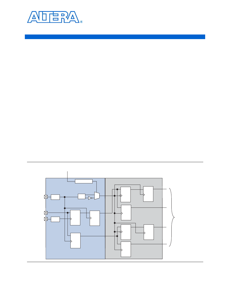
The calibration process of a QDR II+/QDR II SRAM device is considerably simpler
than that of a calibration process for a DDR2/DDR SDRAM device. The calibration
process involves selecting the right phase of the resynchronization clock to capture
the read data at half rate.
shows the generation of the resynchronization
clock which then clocks the HDR registers in the IOE. During calibration, the
sequencer determines whether to use the half-rate clock or the inverted half-rate clock
to capture the half-rate data.
Figure 3–1. Resynchronization Clock in QDR II+/QDR II SRAM ALTMEMPHY Megafunction
CQn
Input from
Sequencer
D
Q
D
Q
Shift Register
1/2
shifted
D
Q
DQ
D
Q
D
Q
D
Q
D
Q
D
Q
D
Q
Half-Rate Data
CQn
shifted