Altera Phase-Locked Loop Reconfiguration IP Core User Manual
Page 36
Page 36
Design Example
Phase-Locked Loop Reconfiguration (ALTPLL_RECONFIG) Megafunction
February 2012
Altera Corporation
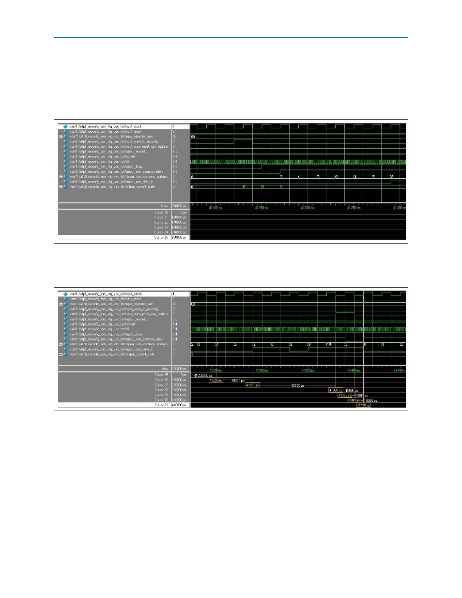
The next part of the simulation demonstrates the PLL reconfiguration from ROM 1
again, but highlights the ROM address resetting capabilities during writing from an
external ROM to the scan cache of the ALTPLL_RECONFIG instantiation. The
c0
signal is 500 MHz and is reconfigured to 100 MHz.
shows the process of
initiating writing the contents of ROM 1 to the ALTPLL_RECONFIG instantiation.
shows how the
reset_rom_address
capability is used.
At 41,250 ns, the
tapout_rom_common_rden
signal is asserted with the
tapout_rom_common_address [7:0]
signal with a value of 4. Observe that the
tapout_busy
signal is asserted. The
output_current_state
signal is
3
. The normal
writing process from ROM to scan cache of the ALTPLL_RECONFIG instantiation
continues.
At 41,290 ns, the
tapout_rom_common_rden
signal is asserted with the
tapout_rom_common_address [7:0]
signal with a value of 6. The
tapout_rom_data_in
signal contains the valid data from address 4 because of the 2-clock-cycle delay. The
tapout_busy
signal is asserted. The
output_current_state
signal is
3
.
At 41,380 ns, the
input_main_reset_rom_address
is asserted for 1 clock cycle. This
signal controls the
reset_rom_address
of the ALTPLL_RECONFIG instantiation. It
resets the address counter in the ALTPLL_RECONFIG instantiation to 0.
Figure 31. Initial Writing from ROM 1 to the Scan Cache of the ALTPLL_RECONFIG Megafunction (41,070 to 41,330 ns)
Figure 32. Resetting the Address when Writing from ROM 1 to the Scan Cache of the ALTPLL_RECONFIG Megafunction
(41,200 to 41,450 ns)