Altera Phase-Locked Loop Reconfiguration IP Core User Manual
Page 34
Page 34
Design Example
Phase-Locked Loop Reconfiguration (ALTPLL_RECONFIG) Megafunction
February 2012
Altera Corporation
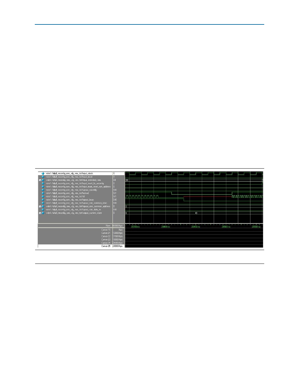
At 10,170 ns, the
tapout_busy
signal remains asserted. The
output_current_state
signal remains at a value of
6
. Therefore, the state machine is still waiting for the
tapout_busy
signal to be deasserted. The
locked
signal is deasserted, which means
the PLL has lock loss, and the
c0
signal is at a
0
value and not producing a clock pulse.
At 10,190 ns, the
tapout_busy
signal is deasserted. This means the PLL
reconfiguration process is complete. The
output_current_state
signal remains at a
value of
6
. The
locked
signal remains deasserted. The
c0
signal is an unknown value
and still not producing a clock pulse.
At 10,210 ns, the
tapout_busy
signal remains deasserted. The
output_current_state
signal changes to a value of
0
. This is the original state, in which the state machine
waits for the next reconfiguration from an external ROM. The
locked
signal remains
deasserted. The
c0
signal is an unknown value and still does not produce a clock
pulse.
At 10,290 ns, the
tapout_busy
signal remains deasserted. The
output_current_state
signal remains at a value of
0
. The
locked
signal is asserted. The
c0
signal now
produces a 200-MHz clock signal, which is the intended setting from ROM 1.
through
show the PLL reconfiguration process from the
remaining ROMs (ROM 2, ROM 3, and ROM 4, respectively).
Figure 28. PLL Reconfiguration from ROM 2 (20,330 to 20,600 ns)
Note to
(1) From
c0
= 200 MHz to
c0
= 300 MHz.