Altera Phase-Locked Loop Reconfiguration IP Core User Manual
Page 28
Page 28
Design Example
Phase-Locked Loop Reconfiguration (ALTPLL_RECONFIG) Megafunction
February 2012
Altera Corporation
7. rom_4:u7—This represents the external ROM, which contains the intended
reconfiguration settings of the PLL. It is has a 1-bit output port (
q
) because of the
serial nature of writing the intended PLL settings to the scan-chain cache of the
pll_reconfig_circuit
module. It has a capacity of 256 words of 1-bit size. The ROM
uses 256 words because that is the closest approximate size of the scan-chain file
for this type of PLL, which is 234 bits. For this ROM, it is represented by the .mif
file the_pll_500_mhz.mif, which is 234 bits. The settings are as follows:
■
inclk
= 50 MHz
■
c0
= 500 MHz
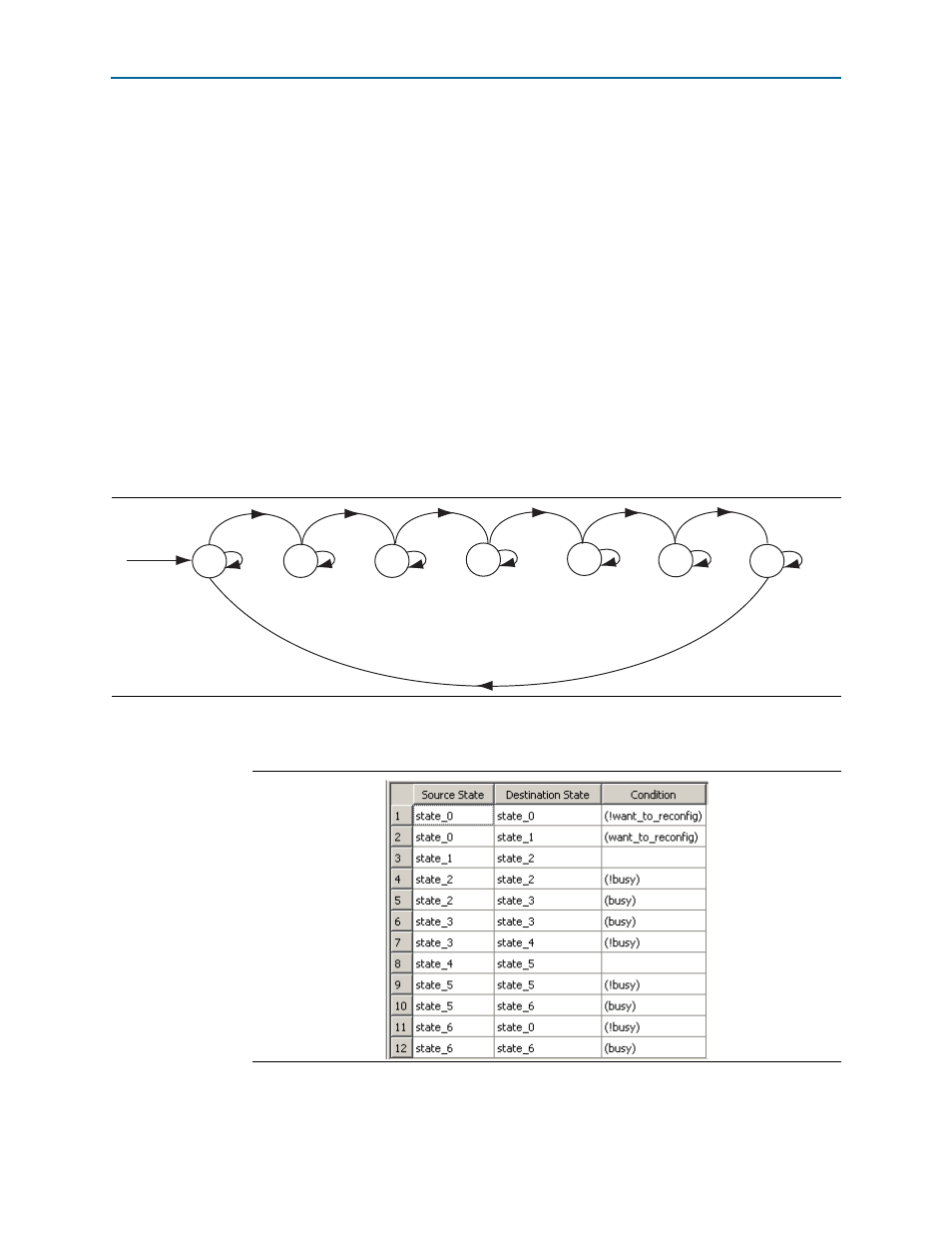
8. control_sm:u8—This represents the state machine that controls the three main
processes involved in the PLL reconfiguration with multiple .mif files via external
ROMs. The state machine selects the ROM to be reconfigured, initiates the writing
of the ROM content to the scan-chain cache, and initiates the reconfiguration of the
PLL using the written content in the scan-chain cache to the PLL. You can modify
this simple state machine to suit your design needs.
shows the state diagram for the state machine.
shows the corresponding condition for the state transition.
Figure 21. Control_sm Module State Diagram
state_0
state_1
state_2
state_3
state_4
state_5
state_6
reset
Figure 22. Control_sm Module State Transition Conditions