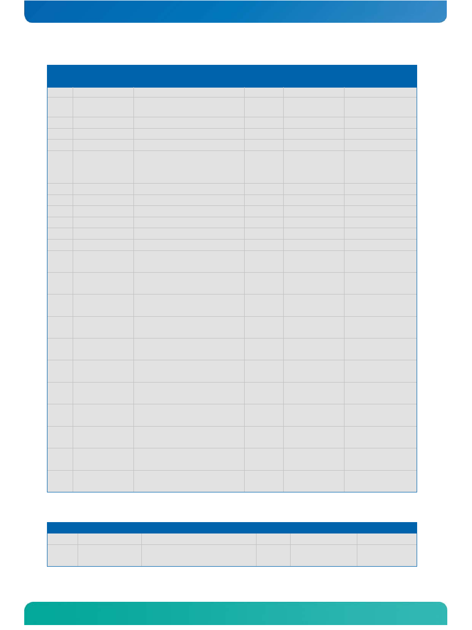
Table4: connector x1a - row b – Kontron COMe-cXLi2 User Manual
Page 25
Kontron COMe-cXLi2 User’s Guide
www.kontron.com
19
Pin
Signal
Description
Type
Terminatio
n
Comment
+
A89
PCIE0_CK_REF
-
PCIe Clock (negative) DP-O
-
100MHz
A90
GND_12
Power Ground
PWR
-
-
A91
RSVD1
Reserved
nc
-
-
A92
RSVD2
Reserved
nc
-
-
A93
SDIO_Clk
GPO0
SDIO#0 Clock
General Purpose
Output 0
O-3.3
O-3.3
PU 75k in
US15W
PD 1k
Bus Switch
PI5C3390
A94
RSVD3
Reserved
nc
-
-
A95
RSVD4
Reserved
nc
-
-
A96
GND_13
Power Ground
PWR
-
-
A97
VCC_12V_1
12V VCC
PWR
-
-
A98
VCC_12V_2
12V VCC
PWR
-
-
A99
VCC_12V_3
12V VCC
PWR
-
-
A10
0
GND_14
Power Ground
PWR
-
-
A10
1
VCC_12V_4
12V VCC
PWR
-
-
A10
2
VCC_12V_5
12V VCC
PWR
-
-
A10
3
VCC_12V_6
12V VCC
PWR
-
-
A10
4
VCC_12V_7
12V VCC
PWR
-
-
A10
5
VCC_12V_8
12V VCC
PWR
-
-
A10
6
VCC_12V_9
12V VCC
PWR
-
-
A10
7
VCC_12V_10
12V VCC
PWR
-
-
A10
8
VCC_12V_11
12V VCC
PWR
-
-
A10
9
VCC_12V_12
12V VCC
PWR
-
-
A11
0
GND_15
Power Ground
PWR
-
-
Table4: Connector X1A - Row B
Pin
Signal
Description
Type
Termination Comment
B1
GND_16
Power Ground
PWR
-
-
B2
GBE0_ACT#
Ethernet Activity LED
O-3.3 Buffered
3.3V Output
-