Elecraft XV Assembly Manual for XV432 MHz User Manual
Page 34
- 32 -
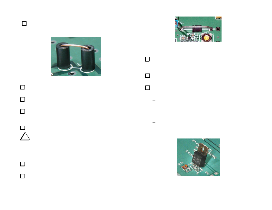
Locate the solder pads for choke L7 on the left side of the PCB next
to electrolytic capacitor C26 near the notch. Choke L7 consists of a bare
wire passing through two ferrite beads as shown in Figure 20.
Figure 20. Installing L7.
Strip the insulation from 3” (7.5 cm) of the #24 solid insulated wire
provided.
Bend the wire into a U shape to match the spacing of the holes on
the PCB. Place a bead on either side of the bend.
Thread the ends of the wires through the solder pads for L7. Make
sure the beads are sitting vertically on the PCB over each hole and bend
the leads on the bottom of the PCB to hold the assembly in place.
Solder both leads and trim them as short as possible.
i
After removing the temporary jumper in the following steps,
amplifier Q3 will be exceptionally vulnerable to ESD damage until L1
is in place. Take ESD precautions (see page 5). Wear a grounded
wrist strap or, as a minimum, touch an unpainted, grounded object
before touching the PCB.
Cut a 1-1/4 inch (3.2 cm) length of the bare 16 gauge tinned wire
provided. Use your needle nose pliers to straighten the wire.
Remove the temporary jumper from the position for L1, then shape
the 16-gauge wire to fit between the pads for L1 (upper left quadrant) as
shown in Figure 21. Use one of the terminal shorting blocks lying on its
side to space the wire above the PCB.
Figure 21, Inductor L1 Positioned for Soldering.
Shorting Block on Its Side Provides Proper Spacing.
Ensure the wire is parallel to the PCB and spaced away from it by
the thickness of the shorting block, then solder it in place from the top
of the PCB. Take care not to touch or R13 or C1 with your iron.
Remove the shorting block, turn the PCB over and clip the excess
leads as short as possible.
Install transistor Q4 (620) in the space provided near diodes D7
and D8 in the lower right quadrant as follows:
Orient the tab over the heavy line on the silkscreen outline,
and insert the transistor up to the shoulders on the leads.
Bend the leads to hold the transistor in place, then solder trim
the leads on the bottom of the PCB.
Tilt the transistor back at an angle so the top is not more than
7/8” (2.2 cm) above the PCB to provide clearance between
the tab and the transverter cover when the unit is assembled.
(See Figure 22).
Figure 22. Installing Transistor Q4.