Elecraft XV Assembly Manual for XV432 MHz User Manual
Page 30
- 28 -
Install the capacitors listed below near the circle for OV1 between
the upper and lower right quadrants.
__C14, 15 pF (15) or (150)
__C14A, 15 pF (15) or (150)
Install monolithic capacitor C12, 18 pF (18) or (180) near the circle
for OV1 between the upper and lower right quadrants.
Install the monolithic capacitors listed below. Start with C71 on the
edge of the PCB in the lower right quadrant and work from right to left
across the lower part of the PCB.
__C71,.01
F (103)
__C57, 100 pF (101)
__C19, .01
F (103)
Install disc ceramic capacitor C18, 4.7 pf (4.7) near C17 in the lower
right quadrant of the PCB.
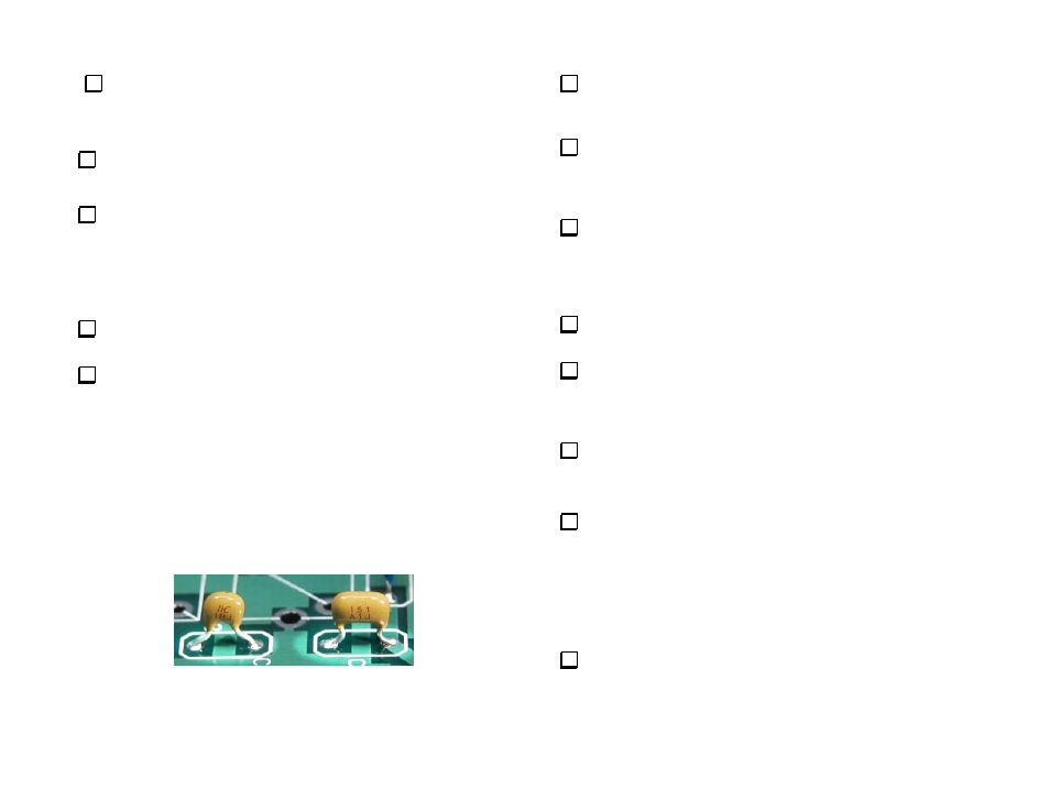
Install the capacitors listed below in the lower right quadrant in the
area marked
28 MHZ IF BANDPASS FILTER
. The lead spacing of these
capacitors may be narrower than the hole spacing on the PCB. If
necessary, form the leads to avoid stress on the capacitor when they are
inserted in the PCB. Do not force the capacitors down against the PCB.
Capacitors with lead spacing narrower than the hole spacing may sit about
1/16” (1.5 mm) above the PCB as shown in Figure 17 .
__C55, 180 pF (181)
__C54, 150 (151) pF
__C53, 22 pF (220) or (22)
__C52, 150 (151) pF
__C56, 180 pF (181)
The capacitors shown are typical.
Other styles may be supplied.
Figure 17. Installing I.F. Filter Capacitors.
Locate the rectangular 2-6 pF trimmer capacitor C1. Turn the
trimmer over and note that there is a small dot near one of the
terminals.
Install C1 in the space provided in the upper left quadrant with
the terminal nearest the dot toward the space for L1. The outline on the
PCB may not match the shape of the trimmer. The temporary jumper
across the solder pads for L1 should still be in place on the PCB.
Use a discarded lead to create test point TP3. Two solder pads for
TP3 are directly below SMD resistor R17 in the upper right quadrant
of the PCB. Bend the lead in a “U” shape and insert it in the pads
indicated with a line between them on the PCB. The loop formed
should rise about 1/4” (4 mm) above the PCB. Solder the leads.
Use a discarded lead to create TP4 next to TP3, following the
procedure described above. Solder the leads.
Make two ground test points just like you did for TP3 and TP4.
Install them where indicated by ground symbols. One location is in the
lower right quadrant above the “Elecraft” label and the other is in the
lower left quadrant near the left edge of the PCB. Solder the leads.
Remove seven of the eight small relays (G6E-134P) from the
carrier tube. If any of the pins are bent, straighten them carefully using
long-nose pliers.
Place the relays below at the locations shown. They can only be
installed one way. Do not solder the relays yet and do not clip or bend
the relay leads.
Upper
Right:
__K8 __K9
__K7 __K4 __K5 __K6
Lower
Left:
__K2
Note that K1 is not installed at this time. It will be installed later.
Use a thin, hardcover book to hold the relays in place, then flip
the PCB and book over together.