Elecraft XV Assembly Manual for XV432 MHz User Manual
Page 22
- 20 -
i
The front panel PCB has parts on both sides of the PCB.
Follow the instructions carefully. If parts are placed on the wrong
side of the PCB, it will not mate with the RF PCB properly or it will
not fit inside the enclosure when construction is finished. Parts that
go on the back (not silk screened) side of the PCB are identified by
asterisks on the silk screening.
Place the 28 pin IC socket in the holes provided at the end of the
front panel PCB opposite the light bar you just installed. The socket goes
on the BACK of the PCB (the side opposite the silk-screened outline).
Orient the socket so the notch in the end is facing away from the end of
the PCB, as shown on the outline.
While holding the IC socket against the PCB, wet the tip of your
soldering iron with a very small amount of solder and then touch it to a
pin and solder pad at one end of the socket to tack-solder it in place.
Tack-solder a second pin at the opposite end of the socket.
Check the IC socket carefully to ensure:
The socket is on the side of the PCB that is not silk-screened.
The notched end of the socket is on the end farthest from the end
of the PCB (as shown on the silk-screened outline).
The socket is against the PCB at both ends. If necessary, heat the
tack-soldered joints and adjust the socket so it is flush.
Solder all 28 pins of the IC socket and trim the leads. Be sure to
solder properly the two pins you tack-soldered above.
i
If your solder joints are not clean and shiny, your iron may
not be hot enough, or you may be using the wrong type of solder.
These "cold" solder joints will likely result in poor performance,
reliability problems, or component failure. You may wish to consult
our web site for additional soldering instructions and tool
recommendations.
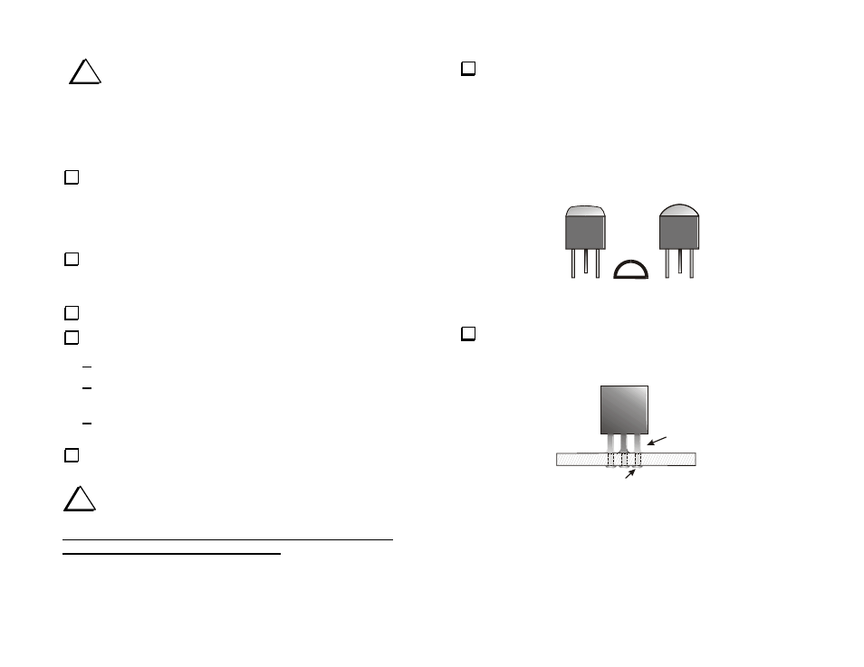
Locate the silk-screened outline for Q5 near the yellow light bar.
Install a PN2222 transistor on the back side of the PCB (the side that is
not silk-screened). The transistor’s leads should protrude through the
PCB on the silk-screened side.
Note: The wide, flat side of the transistor must line up with the flat
side of the silk-screened outline on the PCB (See Figure 7). The
part number may be on either side of the transistor.
OR
FLATTENED
BACK
ROUNDED
BACK
PCB OUTLINE
Figure 7. Transistor Orientation Guide.
Position the transistor on the PCB as shown in Figure 8 and bend
the leads to hold it in place. Solder and trim the leads as short as
possible.
APPROX.
3/16” (3 mm)
SPACE
SOLDER & TRIM LEADS
Figure 8. Installing Transistors.