Common/synth lane receive equalization registers, Pma transmit control registers, Tx/rx lane transmit control registers – Achronix Speedster22i 10G/40G/100G Ethernet User Manual
Page 96
96
UG029, September 6, 2013
Common/Synth Lane Receive Equalization Registers
Table 59
– Common/Synth Lane Receive Equalizer Control Registers
Reg
Pg.
(hex)
Reg Offset [Start
Bit: End Bit]
(hex)
Register Field Name
Reg
Type
RW/R
Default
Value
(hex)
Description
4
53[0:0]
RXAGC_DCCOUPLEEN
4
53[1:1]
RXAGC_XCOUPLEAGCE
N
PMA Transmit Control Registers
The following sections describe registers used to control the transmit levels within the PHY.
The Receiver/Transmitter and Synthesizer control registers are split into the two sub-sections.
TX/RX Lane Transmit Control Registers
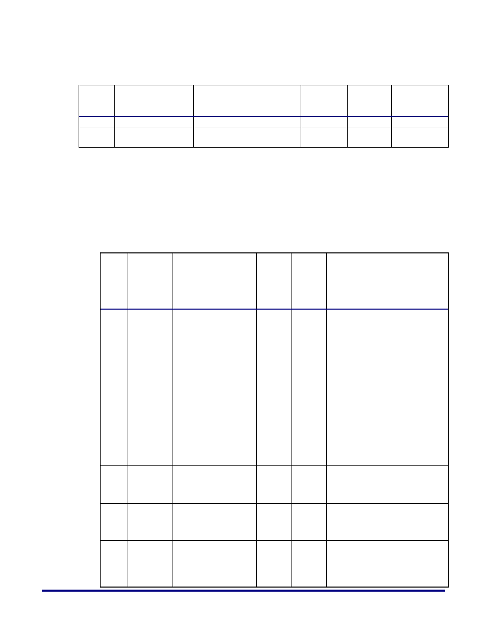
Table 60
– TX/RX Lane Transmit Driver Control Registers
Reg
Page
(hex)
Reg
Offset
[Start
Bit: End
Bit]
(hex)
Register Field
Name
Reg
Type
(RW/R)
Default
Value
(hex)
Description
0
15[2:0]
TXDRV_HLEV
RW
5
Transmit Amplitude control
signal. Used to define the full-
scale maximum swing of the
driver.
000 - Not Supported
001 - 952mVdiff-pkpk
010 - 1024mVdiff-pkpk
011 - 1094mVdiff-pkpk
100 - 1163mVdiff-pkpk
101 - 1227mVdiff-pkpk
110 - 1283mVdiff-pkpk
111 - 1331mVdiff-pkpk
Equivalent to
ICTL_PCS_TXAMP_Lx_[2:0]
interface pin.
Refer to Section 2.6 for further
information.
0
15[7:3]
TXDRV_LEVN
RW
13
Defines the total number of
driver units allocated to the sum
of the driver taps. The
maximum value is 5’h1b.
0
16[3:0]
TXDRV_LEVNM1
RW
2
Defines the total number of
driver units allocated to the first
post-cursor (C+1) tap. The
maximum value for C
+1
is 4’h9.
0
16[5:4]
TXDRV_LEVNM2
RW
0
Defines the total number of
driver units allocated to the
second post-cursor (C+2) tap.
The maximum value for C
+2
is
2’h3.