Pma registers, Pma state control, Memory bus (membus) interface – Achronix Speedster22i 10G/40G/100G Ethernet User Manual
Page 93: Memory address decoding, Pma receive equalization registers
UG029, September 6, 2013
93
PMA Registers
The PMA memory contains control registers which can be grouped into two main categories:
PMA Transmitter/Receiver Control – 1 page of memory.
PMA Synthesizer/Common Control – 1 page of memory.
The PHY module includes many control registers are a majority of them operate as override
registers. Changing these register values will override local FSM control values or interface
pins. The complex interaction of these registers is automatically managed for the user in the
Achronix 10/40/100G Ethernet Core software IP wizard.
PMA State Control
Memory Bus (Membus) Interface
For access to the internal PMA (SerDes) registers, the SBUS is used to access the internal
PMA memory bus (Membus).
The synchronous Membus control port consists of two internal registers: a 16-bit Address
Register and an 8-bit Data Register, as well as control signals to perform register reads and
writes. The Membus is active in all power states, except for when POR is asserted.
This interface to the Memory Bus Interface is provided through the serial SBUS interface
Memory Address Decoding
The PMA memory is partitioned into 2 pages of memory – called Page 0 and Page 4. Page 4
consists of common registers that are applied to all lanes. Page 0 consist of unique registers
for Lanes 0 – 3 of a SerDes quad. The following memory address format is used for
identifying the Memory Page and Offset during a read or write transaction:
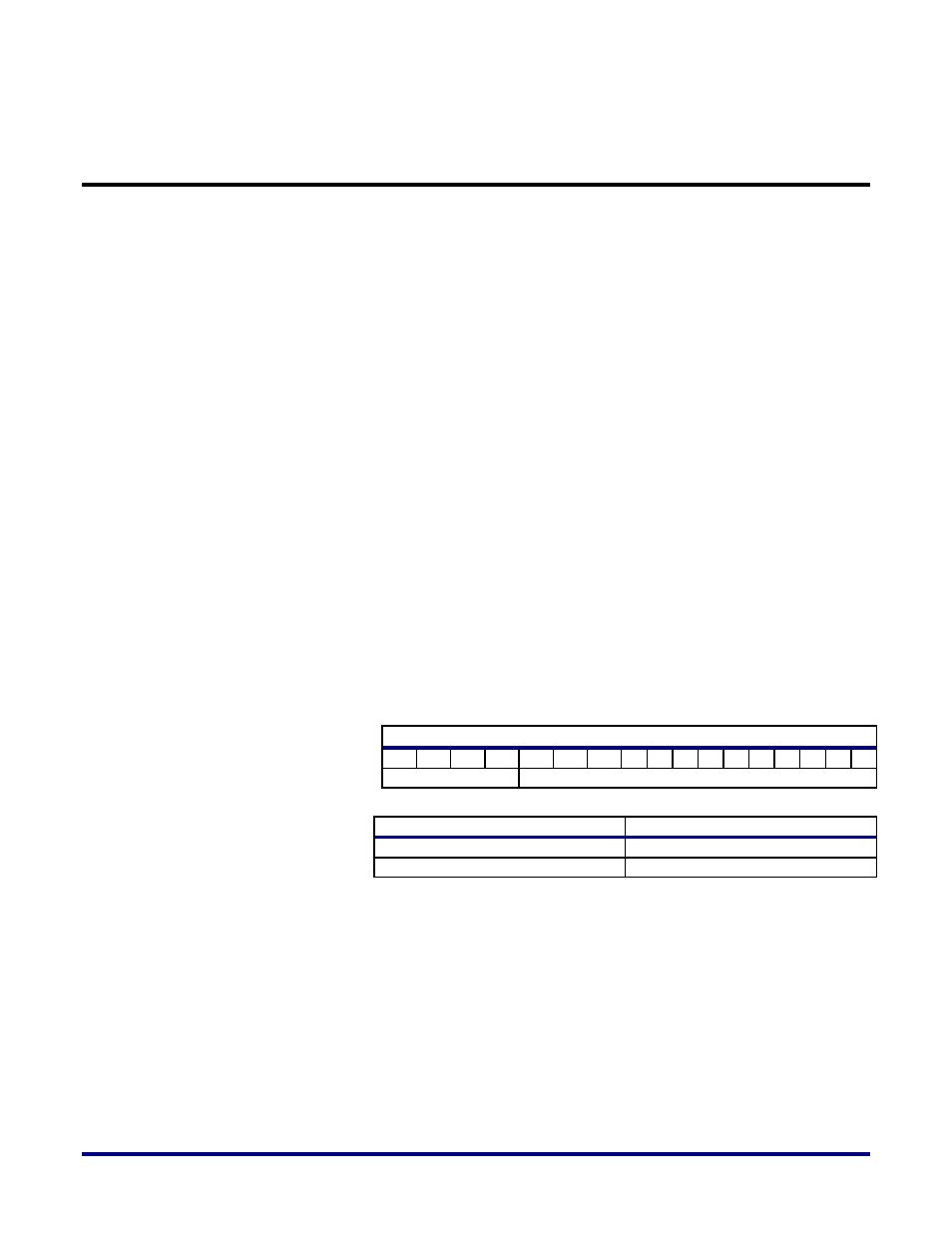
Table 57
– Memory Address Format
ICTL_PCS_MEM_ADDR_[15:0]
16 15 14 13 12 11 10 9 8 7 6 5 4 3 2 1 0
Page Select
Offset Select
Memory Page Select Address Decode
Page Select
3’b1000
Selects Page 0
– Lane 0 - 11
3’b1100
Selects Page 4
– Common Lane
PMA Receive Equalization Registers
The following sections describe registers used to configure the Receive Equalization within
the Receiver in the PHY. The Receiver/Transmitter and Synthesizer control registers are split
into the two sub-sections.
Note: The Register offsets for the PMA control registers are indexed to a base address of
17’h10000