3 connection between fgv and host, 3 analog output, 4 overload/comparator output – SHIMPO FGV-XY-Series User Manual
Page 28
-27-
6.2.3 Connection between FGV and Host
Without the connection between the Digital GND and
pin 5, RS-232C communication will not work.
6.3 Analog Output
± 1V Analog Output
The output voltage's polarity corresponds to the polarity shown on the display during standard measurement mode.
The voltage will adjust to any tare command performed.
Output signal
± 1V
Signal method
12 bit D/A converter
Output update
1000 times/second*
Load resistance
>10 k Ω
Output accuracy
± 50mV
The analog output has a default update rate of 1000 times/second. The output
voltage is linearly scaled so that the current zero point of the gauge corresponds
with 0V, and so that 1V corresponds with 100% of the gauge's rated capacity.
This means that the tare function, or any change in the gauge's zero point, will
change the maximum voltage shown before the gauge is overloaded.
6.4 Overload/Comparator Output
Output overload/comparator signal.
Switch of output overload/comparator signal is set by external output setting (f06) of function mode.
Compression Overload /
LO Comparator Trigger
Tension Overload /
HI Comparator Trigger
Common
(For Pins 8 and 9)
30V / 5mA Maximum
Overload Output
When the overload condition is triggered, the corresponding overload output turns on. This can be used to stop a motorized test stand, or an
alarm to prevent damage from accidental overload.
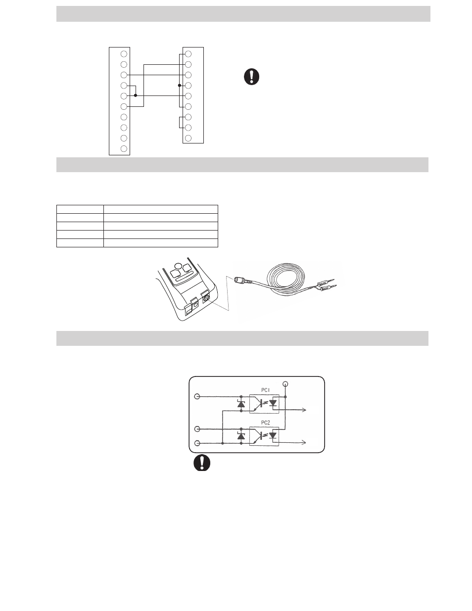
When compression overload occurs photo-couple 1(PC1) turns on, and allows current to fl ow between Pin 8 and 10.
When tension overload occurs photo-couple 2(PC2) turns on, and allows current to fl ow between Pin 9 and 10.
If no overload condition exists, PC1 and PC2 should be closed, and will not allow current fl ow.
Overload occurs at about 120% of the gauge's rated capacity. This includes any weight zeroed during any tare operation.
Comparator Output
When the LO limit is reached, photo-couple 1(PC1) turns on, and allows current to fl ow between pins 8 and 10.
When the HI limit is reached, photo-couple 2(PC2) turns on, and allows current to fl ow between pins 9 and 10.
Refer to section 5.5 for information regarding the activation and setting of comparator limits.
I/F Circuit
1
2
3
4
5
6
7
8
9
10
1
2
3
4
5
6
7
8
9
RxD
TxD
Digital GND
Connection Detection
FGV
Data Ouput Port
Host
9 pin serial connection
Analog Cable
(Optional)
Red
Black
+
-
Pin 8
Pin 9
Pin 10
DCD
RxD
TxD
DTR
GND
DSR
RTS
CTS
RI
*This rate is determined by setting f05. Please refer to 4.5.5.