Cn7 / cn13, Table 12 - spi header pin out, Figure 4 - spi header – B&B Electronics WLNN-EK-DP551 - User Manual User Manual
Page 18
B&B Electronics
18
Airborne Enterprise WLNN EVB Users Guide
Designator
Pin
Description
5
TDI: Test Data In
6
GND
7
TMS: Test Mode Select
8
GND
9
TCK: Test Clock
10
GND
11
RTCK: Return Test Clock
12
GND
13
TDO: Test Data Out
14
GND
15
/RESET (Active Low)
16
GND
17
No Connect
18
GND
19
No Connect
20
GND
Use of this header requires that JTAG has been enabled on the Airborne Device Server
Module. Production devices do not support this feature.
To enable JTAG a hardware change to the module must be made, please contact
B&B Electronics Technical Support if this feature is required.
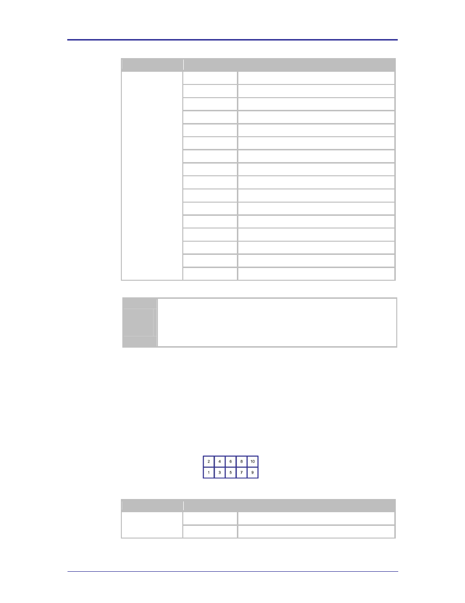
5.10 CN7 / CN13
Header CN7 is the primary SPI interface header; firmware selection of the SPI
interface is required before the interface can be used. CN13 allows a secondary
connection to the SPI interface. CN7 and CN13 have common connections.
The header pin out can be seen in Figure 4 and Table 12.
FIGURE 4 - SPI HEADER
TABLE 12 - SPI HEADER PIN OUT
Designator
Pin
Description
CN7
1
No Connect
2
GND