Rainbow Electronics DS2143Q User Manual
Page 24
DS2143/DS2143Q
031397 24/40
Sa5
TNAF.3
Additional Bit 5.
Sa6
TNAF.2
Additional Bit 6.
Sa7
TNAF.1
Additional Bit 7.
Sa8
TNAF.0
Additional Bit 8.
12.0 LINE INTERFACE CONTROL FUNCTION
The DS2143 can control line interface units that contain
serial ports. When Control Register Bytes 1 or 2 (CRB1,
CRB2) are written to, the DS2143 will automatically
write this data serially (LSB first) into the line interface by
creating a chip select, serial clock and serial data via the
LI_CS, LI_SCLK and LI_SDI pins respectively. This
control function is driven off of the RCLK and it must be
present for proper operation. Registers CRB1 and
CRB2 can only be written to, they cannot be read from.
Writes to these registers must be at least 20
µ
s apart.
See Section 13 for timing information.
CRB1: CONTROL REGISTER BYTE 1 (Address=18 Hex)
CRB2: CONTROL REGISTER BYTE 2 (Address=19 Hex)
(MSB)
(LSB)
CR7
CR6
CR5
CR4
CR3
CR2
CR1
CR0
CR7
CR6
CR5
CR4
CR3
CR2
CR1
CR0
SYMBOL
POSITION
NAME AND DESCRIPTION
CR1
CRB1.0
LSB of Control Register Byte 1
CR7
CRB2.7
MSB of Control Register Byte 2
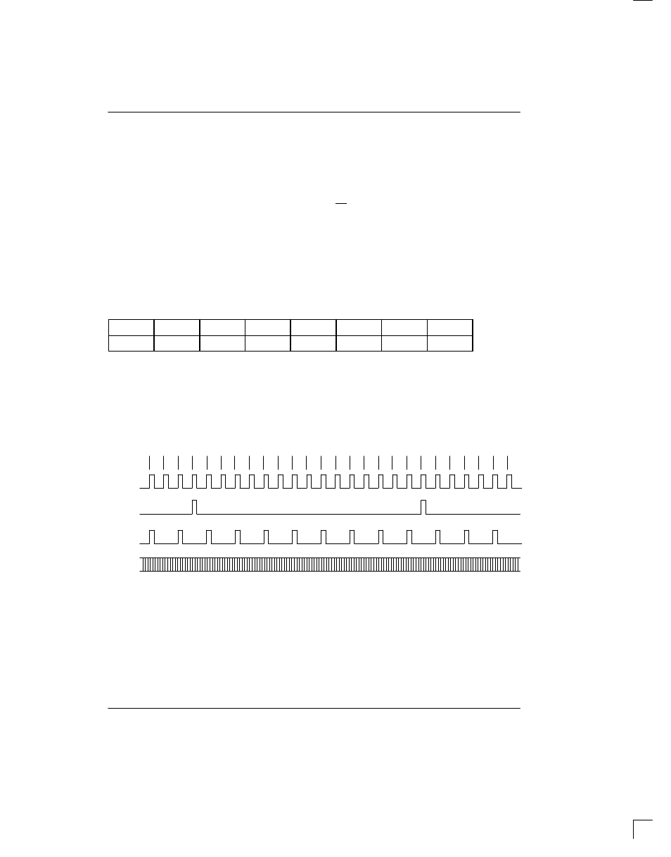
13.0 TIMING DIAGRAMS
RECEIVE SIDE TIMING
15 16
1
2
3
4
5
6
7
8
9
10 11 12
13 14 15
FRAME#
16
1
2
3
4
5
6
14
RSYNC
1
RSYNC
2
RCLK
3
RLINK
4
NOTES:
1. RSYNC in the frame mode (RCR1.6=0).
2. RSYNC in the multiframe mode (RCR1.6=1).
3. RLCLK is programmed to output just the Sa4 bit.
4. RLINK will always output all five Sa bits as well as the rest of the receive data stream.
5. This diagram assumes the CAS MF begins with the FAS word.
CRB1
CRB2