Rainbow Electronics DS2141A User Manual
Page 3
DS2141A
021997 3/35
DS2141A FEATURES
•
parallel control port
•
large error counters
•
onboard dual 2–frame elastic store
•
FDL support circuitry
•
robbed–bit signaling extraction and insertion
•
programmable output clocks
•
fully independent transmit and receive sections
•
frame sync generation
•
error–tolerant yellow and blue alarm detection
•
output pin test mode
•
payload loopback capability
•
SLC–96 support
•
remote loop up/down code detection
•
loss of transmit clock detection
•
loss of receive clock detection
•
1’s density violation detection
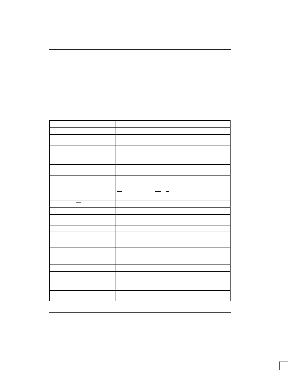
PIN DESCRIPTION Table 1
PIN
SYMBOL
TYPE
DESCRIPTION
1
TCLK
I
Transmit Clock. 1.544 MHz primary clock.
2
TSER
I
Transmit Serial Data. Transmit NRZ serial data, sampled on the
falling edge of TCLK.
3
TCHCLK
O
Transmit Channel Clock. 192 KHz clock which pulses high during
the LSB of each channel. Useful for parallel–to–serial conversion of
channel data, locating robbed–bit signaling bits, and for blocking
clocks in DDS applications. See Section 13 for timing details.
4
5
TPOS
TNEG
O
Transmit Bipolar Data. Updated on rising edge of TCLK.
6–13
AD0–AD7
I/O
Address/Data Bus. An 8–bit multiplexed address/data bus.
14
BTS
I
Bus Type Select. Strap high to select Motorola bus timing; strap low
to select Intel bus timing. This pin controls the function of the
RD(DS), ALE(AS), and WR(R/W) pins. If BTS=1, then these pins
assume the function listed in parenthesis ().
15
RD(DS)
I
Read Input (Data Strobe).
16
CS
I
Chip Select. Must be low to read or write the port.
17
ALE(AS)
I
Address Latch Enable (Address Strobe). A positive–going edge
serves to demultiplex the bus.
18
WR(R/W)
I
Write Input (Read/Write).
19
RLINK
O
Receive Link Data. Updated with either FDL data (ESF) or Fs–bits
(D4) or Z–bits (ZBTSI) one RCLK before the start of a frame. See
Section 13 for timing details.
20
VSS
–
Signal Ground. 0.0 volts.
21
RLCLK
O
Receive Link Clock. 4 KHz or 2 KHz (ZBTSI) demand clock for the
RLINK input. See Section 13 for timing details.
22
RCLK
I
Receive Clock. 1.544 MHz primary clock.
23
RCHCLK
O
Receive Channel Clock. 192 KHz clock which pulses high during
the LSB of each channel. Useful for parallel–to–serial conversion of
channel data, locating robbed–bit signaling bits, and for blocking
clocks in DDS applications. See Section 13 for timing details.
24
RSER
O
Receive Serial Data. Received NRZ serial data; updated on rising
edges of RCLK.