Rainbow Electronics DS2141A User Manual
Page 21
DS2141A
021997 21/35
9.0 CLOCK BLOCKING REGISTERS
The Receive Channel Blocking Registers
(RCBR1/RCBR2/RCBR3) and the Transmit Channel
Blocking Registers (TCBR1/TCBR2/TCBR3) control
the RCHBLK and TCHBLK pins respectively. The
RCHBLK and TCHCLK pins are user–programmable
outputs that can be forced either high or low during indi-
vidual channels. These outputs can be used to block
clocks to a USART or LAPD controller in Fractional T1,
E1 to T1, or ISDN–PRI applications. When the ap-
propriate bits are set to a 1, the RCHBLK and TCHCLK
pins will be held high during the entire corresponding
channel time. See the timing in Section 13 for an
example.
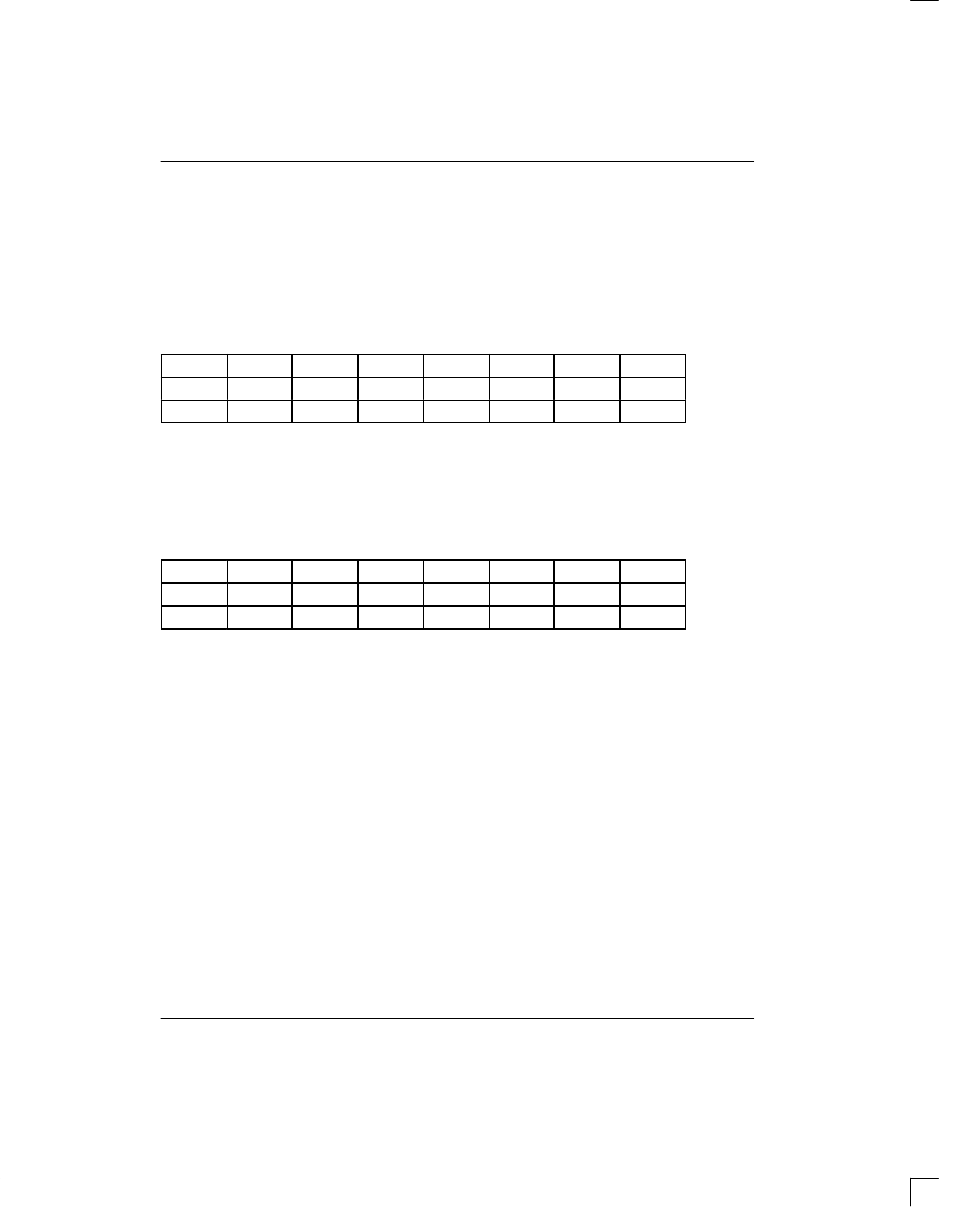
RCBR1/RCBR2/RCBR3: RECEIVE CHANNEL BLOCKING REGISTERS (6Ch to 6Eh)
(MSB)
(LSB)
CH8
CH7
CH6
CH5
CH4
CH3
CH2
CH1
CH16
CH15
CH14
CH13
CH12
CH11
CH10
CH9
CH24
CH23
CH22
CH21
CH20
CH19
CH18
CH17
SYMBOL
POSITION
NAME AND DESCRIPTION
CH24
RCBR3.7
Receive Channel Blocking Registers.
CH1
RCBR1.0
0=force the RCHBLK pin to remain low during this channel time.
1=force the RCHBLK pin high during this channel time.
TCBR1/TCBR2/TCBR3: TRANSMIT CHANNEL BLOCKING REGISTERS (32h to 34h)
(MSB)
(LSB)
CH8
CH7
CH6
CH5
CH4
CH3
CH2
CH1
CH16
CH15
CH14
CH13
CH12
CH11
CH10
CH9
CH24
CH23
CH22
CH21
CH20
CH19
CH18
CH17
SYMBOL
POSITION
NAME AND DESCRIPTION
CH24
TCBR3.7
Transmit Channel Blocking Registers.
CH1
TCBR1.0
0=force the TCHBLK pin to remain low during this channel time.
1=force the TCHBLK pin high during this channel time.
10.0 ELASTIC STORES OPERATION
The DS2141A has two onboard two–frame (386 bits)
elastic stores. These elastic stores have two main pur-
poses. First, they can be used to rate convert the T1
data stream to 2.048 Mbps (or a multiple of 2.048 Mbps)
which is th e E1 rate. Secondly, they can be used to
absorb the differences in frequency and phase between
the T1 data stream and an asynchronous (i.e., not fre-
quency locked) backplane clock. Both elastic stores
contain full controlled slip capability which is necessary
for this second purpose. The receive side elastic store
can be enabled via CCR1.2 and the transmit side elastic
store is enabled via CCR1.7.
10.1 Receive Side
If the receive side elastic store is enabled (CCR1.2 = 1),
then the user must provide either a 1.544 MHz (CCR1.3
= 0) or 2.048 MHz (CCR1.3 = 1) clock at the SYSCLK
pin. The the user has the option of either providing a
frame sync at the RFSYNC pin (RCR2.3 = 1) or having
the RFSYNC pin provide a pulse on frame boundaries
(RCR2.3 = 0). If the user wishes to obtain pulses at the
frame boundary, then RCR2.4 must be set to zero and if
the user wishes to have pulses occur at the multiframe
boundary, then RCR2.4 must be set to one. If the user
selects to apply a 2.048 MHz clock to the SYSCLK pin,
then the data output at RSER will be forced to all ones
every fourth channel and the F–bit will be deleted.
Hence channels 1, 5, 9, 13, 17, 21, 25, and 29 (timeslots
0, 4, 8, 12, 16, 20, 24, and 28) will be forced to a one.
Also, in 2.048 MHz applications, the RCHBLK output
will be forced high during the same channels as the
RSER pin. See Section 13 for more details. This is use-
ful in T1 to CEPT (E1) conversion applications. If the
RCBR1 (6C)
RCBR2 (6D)
RCBR3 (6E)
TCBR1 (32)
TCBR2 (33)
TCBR3 (34)