At83c26 – Rainbow Electronics AT83C26 User Manual
Page 6
6
7511B–SCR–10/05
AT83C26
38
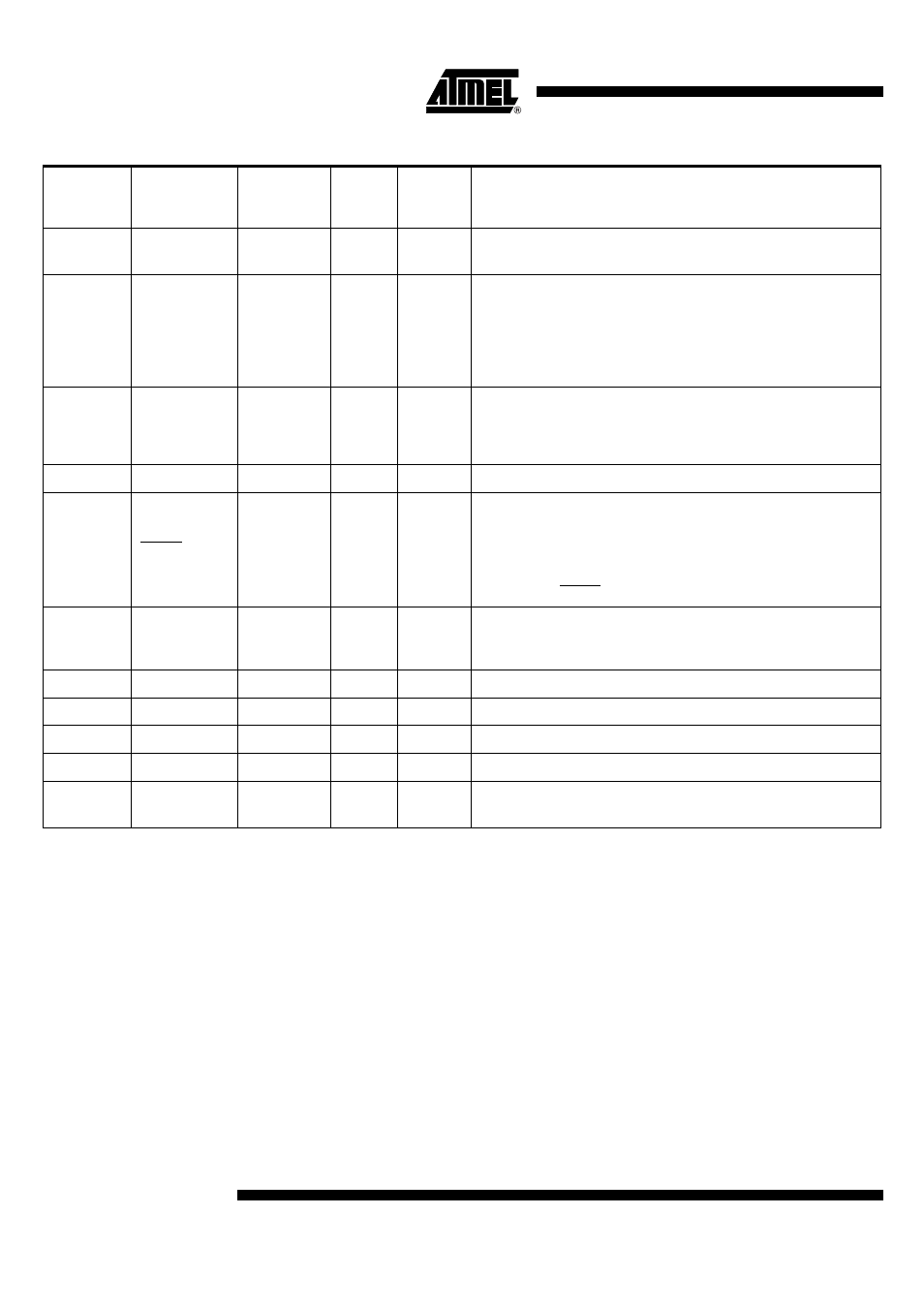
CVSSB
GND
DC/DCB input.
This pin must be directly connected to the VSS of power supply.
39
LIB
2kV
PWR
DC/DCB input.
LIB must be tied to VCC pin through an external coil (typically 10µH) and
provides the current for the charge pump of the DC/DCB converter.
It may be directly connected to VCC if the step-up converter is not used
(see STEPREGB bit in DCDCB register and see minimum VCC values in
Table 53.for class A and Table 54. for class B)
40
CVCCB
2kV
PWR
DC/DCB output.
The two CVCCB pins are connected together near the package. CVCCB
pin is only used for DC/DCB voltage measurements.The reason of two
CVCCB pins is to reduce noise.
41
CVCCB
2kV
PWR
DC/DCB output.
42
RESET
VCC
2kV
I/O
open drain
Micro controller interface function: reset signal.
•
power on reset
•
A low level on this pin keeps the AT83C26 under reset even if
applied on power-on. It also resets the AT83C26 if applied when the
AT83C26 is running.
•
Asserting RESET
43
CPRES2
VCC
4kV+
I
pull up
Card presence for SC2 interface.
An internal pull to VCC can be activated in the pad if necessary using
PULLUP2 bit in SC2_CFG1 register (activated by default).
44
CVCCINB
PWR
This pin must be connected to CVCCB pins next to the package.
45
CVCC2
4kV+
PWR
VCC pin for SC2 interface.
46
CRST2
CVCC2
4kV+
O
CRST pin for SC2 interface.
47
CCLK2
CVCC2
4kV+
O
CCLK pin for SC2 interface.
48
CIO2
CVCC2
4kV+
I/O
pull up
CIO pin for SC2 interface.
Table 1. Ports Description (Continued)
VQFP48 or
QFN48
Pin number
Pad Name
Pad Internal
Power Supply
ESD
Limits
Pad Type
Description