At83c26, Dcdc converters, Clock controller – Rainbow Electronics AT83C26 User Manual
Page 13
13
7511B–SCR–10/05
AT83C26
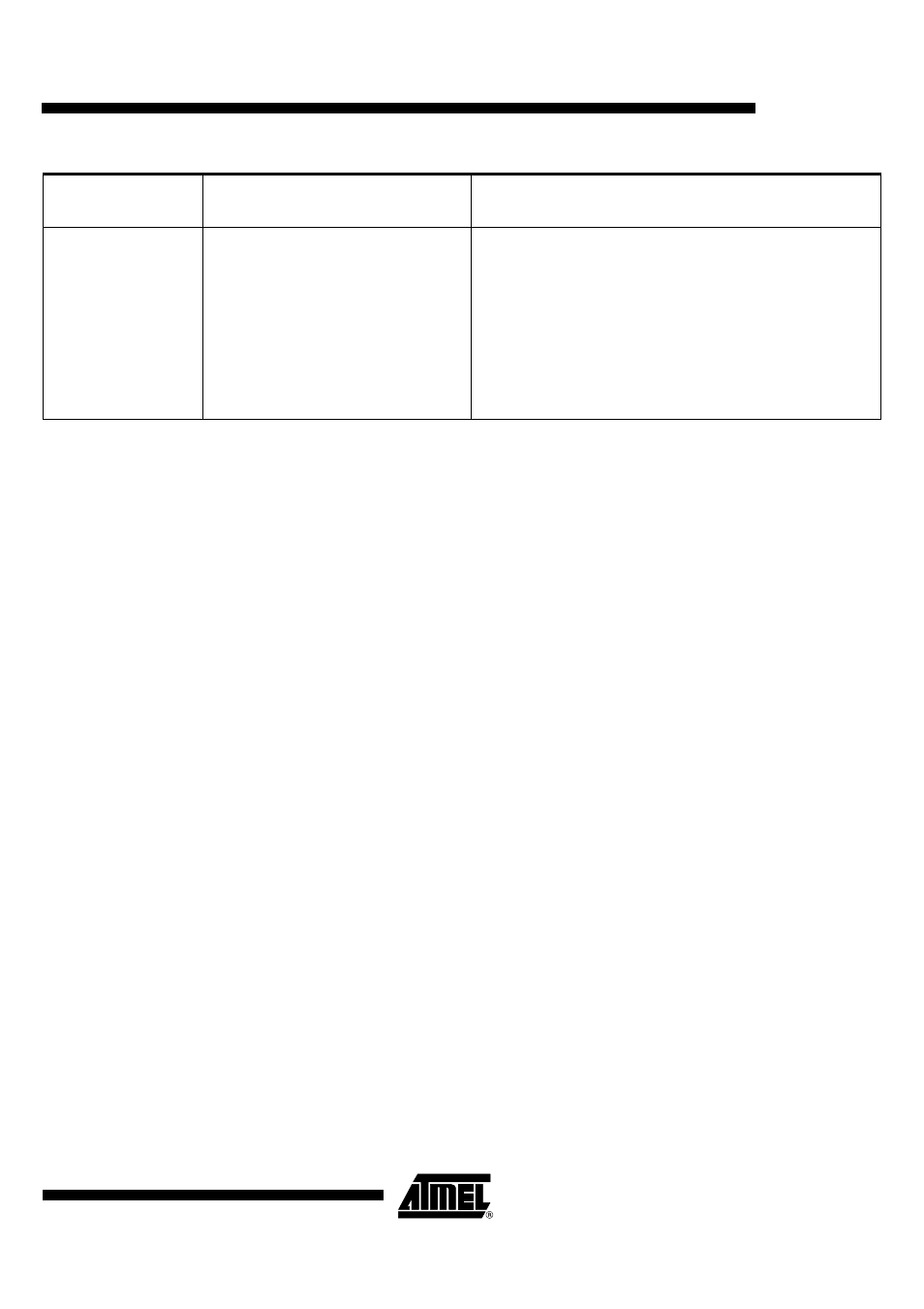
Table 3. SC2 and SC3 shared IOs
DCDC Converters
The DC/DC A converter is used to provide smart card voltage for the SC1 interface (CVCC1).
The DC/DC B converter is used to provide smart card voltage for the SCn interfaces (n=2, 3, 4,
5).
DC/DC converters need a clock of 4MHz (see Section “Clock Controller”). Two internal oscilla-
tors (one for each converter) provide the DC/DC clocks.
The DC/DCB output is connected on 4 LDO regulators (Low Drop Output) to generate CVCCn
voltage (n=2, 3, 4, 5).
Clock Controller
The clock controller outputs six clocks:
1.
Five clocks for CCLK1, CCLK2, CCLK3, CCLK4 and CCLK5. Four different sources can
be used: CLK pin, DCCLK signal, CARDCKn bit (n=1, 2, 3, 4, 5) or A2/CK.
2.
A DCCLK clock used for pads and deactivation sequence.
Clock controller for SCn (n=1, 2, 3, 4, 5)
The transparent mode with A2/CK pin is available on SCn interface. The CKSn[2:0] register is
used to select this transparent mode between A2/CK and CCLKn. The bit CKSTOPn must be
cleared to have CCLKn running according to CKSn[2:0].
Pin name
SC2_FULL = 1
SC3 interface not available
SC2_FULL = 0
SC2 without CC4and CC8 + SC3 interface
CPRES2
CRST2
CIO2
CCLK2
CRST3/CC82
CIO3/CC42
CCLK3
CPRES2
CRST2
CIO2
CCLK2
CC82
CC42
unused
CPRES2
CRST2
CIO2
CCLK2
CRST3
CIO3
CCLK3