At83c26 – Rainbow Electronics AT83C26 User Manual
Page 5
5
7511B–SCR–10/05
AT83C26
22
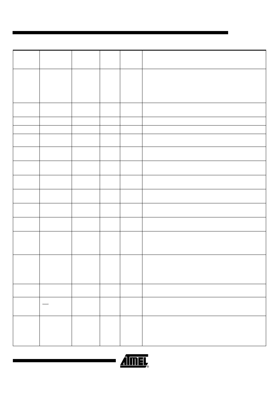
LIA
2kV
PWR
DC/DCA input.
LIA must be tied to VCC pin through an external coil (typically 10µH) and
provides the current for the charge pump of the DC/DCA converter.
It may be directly connected to VCC if the step-up converter is not used
(see STEPREGA bit in SC1_CFG4 register and see minimum VCC
values in Table 50.for class A and Table 51. for class B)
23
CVSS1
2kV
GND
DC/DCA input.
This pin must be directly connected to the VSS of power supply.
24
VCC
2kV
PWR
VCC is used to power the internal voltage regulators and I/O buffers.
25
VSS
2kV
GND
Ground.
26
BYPASS
VCC
2kV
I
A high level on this pin activates a low power consumption mode with
internal regulator bypassed.
27
SDA
VCC
2kV
I/O
open drain
Micro controller interface function: TWI serial data.
An external pull up must be connected on SDA pin (4.7kOhms).
28
SCL
VCC
2kV
I/O
open drain
Micro controller interface function: TWI clock.
An external pull up must be connected on SCL pin (4.7kOhms).
29
IO2
EVCC
2kV
I/O
pull up
The behavior of this pin depends on IOSEL[3/0] bits values (see
IO_SELECT register).
30
IO1
EVCC
2kV
I/O
pull up
The behavior of this pin depends on IOSEL[3/0] bits values (see
IO_SELECT register).
31
AUX2
EVCC
2kV
I/O
pull up
The behavior of this pin depends on IOSEL[3/0] bits values (see
IO_SELECT register).
32
AUX1
EVCC
2kV
I/O
pull up
The behavior of this pin depends on IOSEL[3/0] bits values (see
IO_SELECT register).
33
A1/RST
EVCC
2kV
I
The TWI address depends on the value present on this pin at reset.
If CRST transparent mode is selected, the A1/RST signal is connected to
CRST1 or CRST2 pins (see CRST_SEL1 and CRST_SEL2 bits
respectively in SC1_CFG4 and SC2_CFG2 registers).
34
A2/CK
EVCC
2kV
I
The TWI address depends on the value present on this pin at reset.
If CCLKn transparent mode is selected, the A2/CK signal is connected to
CCLKn pins (with n=1 to 5).
See CKSn[2:0] bits respectively in SC1_CFG1, SC2_CFG2, SC3_CFG2,
SC4_CFG2, SC5_CFG2 registers.
35
CLK
EVCC
2kV
I
Master clock.
36
INT
VCC
2kV
O
open drain
Interruption status.
An internal pull up to VCC can be activated in the pin if necessary using
INT_PULLUP bit in SC1_CFG4 (deactivated by default).
37
EVCC
PWR
Extra supply voltage (Micro controller power supply).
EVCC is used to supply the internal level shifters of host interface pins.
EVCC is connected to the host power supply.
EVCC voltage can be directly connected to VCC if the host power supply
and the AT83C26 power supply is the same.
Table 1. Ports Description (Continued)
VQFP48 or
QFN48
Pin number
Pad Name
Pad Internal
Power Supply
ESD
Limits
Pad Type
Description