At83c26, Signals – Rainbow Electronics AT83C26 User Manual
Page 4
4
7511B–SCR–10/05
AT83C26
Signals
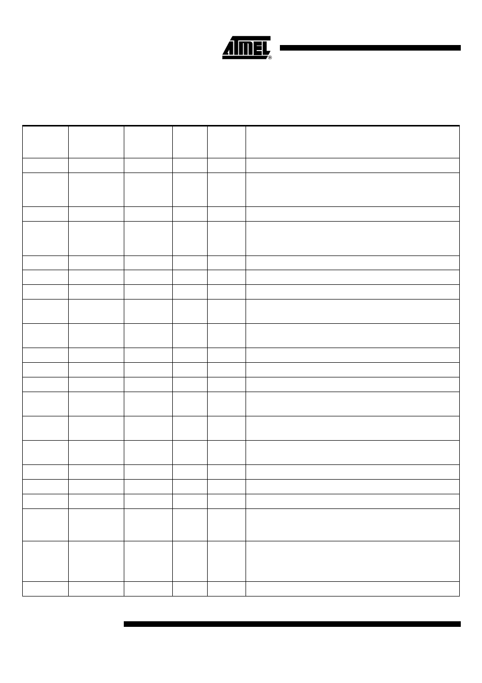
Table 1. Ports Description
VQFP48 or
QFN48
Pin number
Pad Name
Pad Internal
Power Supply
ESD
Limits
Pad Type
Description
1
CVCC3
4kV+
PWR
VCC pin for SC3 interface.
2
CRST3/CC82
CVCC3
4kV+
I/O
pull up
See SC2_CFG1 register:
If SC2_FULL bit = 0, CRST pin for SC3 interface.
If SC2_FULL bit = 1, CC8 pin for SC2 interface.
3
CCLK3
CVCC3
4kV+
O
CCLK pin for SC3 interface.
4
CIO3/CC42
CVCC3
4kV+
I/O
pull up
See SC2_CFG1 register:
If SC2_FULL bit = 0, CIO pin for SC3 interface.
If SC2_FULL bit = 1, CC4 pin for SC2 interface.
5
CVCC4
4kV+
PWR
VCC pin for SC4 interface.
6
CRST4
CVCC4
4kV+
O
RST pin for SC4 interface.
7
CCLK4
CVCC4
4kV+
O
CCLK pin for SC4 interface.
8
CIO4
CVCC4
4kV+
I/O
pull up
CIO pin for SC4 interface.
9
CIO5
CVCC5
4kV+
I/O
pull up
CIO pin for SC5 interface.
10
CCLK5
CVCC5
4kV+
O
CCLK pin for SC5 interface.
11
CRST5
CVCC5
4kV+
O
RST pin for SC5 interface.
12
CVCC5
4kV+
PWR
VCC pin for SC5 interface.
13
CC81
CVCC1
4kV+
I/O
pull up
CC8 pin for SC1 interface.
14
CC41
CVCC1
4kV+
I/O
pull up
CC4 pin for SC1 interface.
15
CIO1
CVCC1
4kV+
I/O
pull up
CIO pin for SC1 interface.
16
CCLK1
CVCC1
4kV+
O
CCLK pin for SC1 interface.
17
CRST1
CVCC1
4kV+
O
RST pin for SC1 interface.
18
CVCCIN1
4kV+
PWR
This pin must be connected to CVCC1 pins next to the package.
19
CPRES1
VCC
4kV+
I
pull up
Card presence for SC1 interface.
An internal pull up to VCC can be activated in the pad if necessary using
PULLUP1 bit in SC1_CFG1 register (activated by default).
20
CVCC1
4kV+
PWR
VCC pin for SC1 interface.
The two CVCC1 pins are connected together near the package. Only one
wire goes to the smart card connector. The reason of two CVCC1 pins is
to reduce noise.
21
CVCC1
4kV+
PWR
VCC pin for SC1 interface.