At83c26 – Rainbow Electronics AT83C26 User Manual
Page 49
49
7511B–SCR–10/05
AT83C26
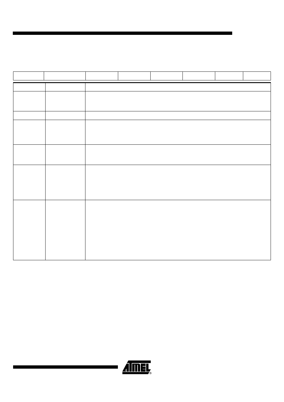
Reset value = 0x 0X00 1000
Notes:
1. When CKS3 value is changed a special logic insures no glitch occurs on the CCLK3 pin and
actual configuration changes can be delayed by half a period to two periods of CCLK3.
2. CCLK3 must be stopped with CKSTOP3 bit before switching from CKS3 = (0, 1, 2, 3, 6, 7) to
CKS3 = (4, 5) or vice versa.
Table 28. SC3_CFG2 ()
7
6
5
4
3
2
1
0
ART3
X
CARDRST3
CARDCK3
CKSTOP3
CK32
CKS31
CKS30
Bit Number
Bit Mnemonic
Description
7
ART3
Automatic Reset Transition
Set this bit to have the CRST3 pin changed according to activation sequence.
Clear this bit to have the CRST3 pin immediately following the value programmed in CARDRST3.
6
X
5
CARDRST3
Card Reset
Set this bit to enter a reset sequence according to ART3 bit value.
Clear this bit to drive a low level on the CRST3 pin.
This bit must be cleared to use AUX2 pin for CRST3 source.
4
CARDCK3
Card Clock
Set this bit to set a high level on the CCLK3 pin (according to CKSTOP3 bit value).
Clear this bit to drive a low level on the CCLK3 pin.
3
CKSTOP3
CARD Clock Stop
Set this bit to stop CCLK3 according to CARDCK3. This can be used to set asynchronous cards in power-
down mode (GSM) or to drive CCLK3 by software.
Clear this bit to have CCLK3 running according to CKS3. This can be used to activate asynchronous cards.
Note:
When this bit is changed a special logic ensures that no glitch occurs on the CCLK3 pin and actual
configuration changes can be delayed by half a period to two periods of CCLK3.
2-0
CKS3[2:0]
Interface 4Card Clock Selection
CKS3 [2:0] = 0: CCLK3 = CLK (then the maximum frequency is 24 MHz)
CKS3 [3:0] = 1: CCLK3 = DCCLK
CKS3 [3:0] = 2: CCLK3 = DCCLK / 2
CKS3 [3:0] = 3: CCLK3 = DCCLK / 4
CKS3 [3:0] = 4: CCLK3 = A2
CKS3 [3:0] = 5: CCLK3 = A2 / 2
CKS3 [3:0] = 6: CCLK3 = CLK / 2
CKS3 [3:0] = 7: CCLK3 = CLK / 4
The reset value is 0.