Rainbow Electronics AT86RF401 User Manual
Page 5
5
AT86RF401
1424D–RKE–09/02
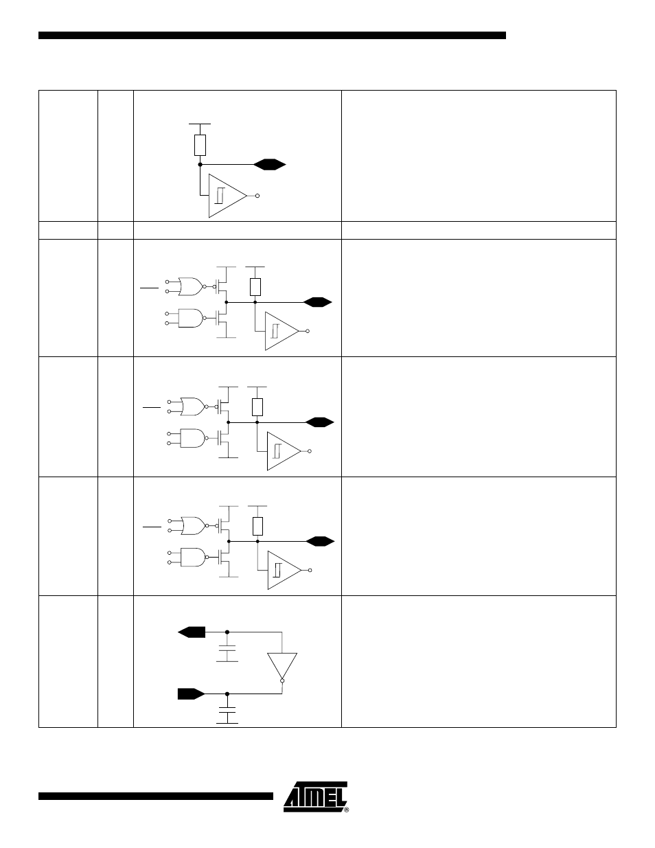
RESETB
5
SPI Reset Input: A “low” on this pin resets the device and puts
the part into SPI mode. A logic-high on this pin causes the
device to execute its program if the V
DD
is above the brown-
out voltage level.
NC
6
No Connect. Float Pin.
I/O0 (SDI)
7
SPI Data In/Input/Output 0: General-purpose I/O and button
input. In SPI mode, this pin serves as SDI (Serial Data Input).
I/O1 (SDO)
8
SPI Data Out/Input/Output 1: General-purpose I/O and button
input. In SPI mode, this pin serves as SDO (Serial Data
Output).
I/O2 (SCK)
9
SPI Clock/Input/Output 2: General-purpose I/O and button
input. In SPI mode, this pin serves as SCK (SPI Clock Input).
XTAL/CLK
10
Crystal/Clock Input: Input to the inverting oscillator amplifier
and input to the internal clock operating circuit. This pin may
be driven externally for test purposes.
Table 2. Pin Descriptions – 20-lead TSSOP (Continued)
V
DD
35 k
Ω
5
To AVR
V
DD
V
DD
Data
Enable
−
Data
Enable
7
35 k
Ω
To AVR
V
DD
V
DD
Data
Enable
−
Data
Enable
8
35 k
Ω
To AVR
V
DD
V
DD
Data
Enable
−
Data
Enable
9
35 k
Ω
To AVR
40 pF
40 pF
10
11