Data eeprom access from the avr – Rainbow Electronics AT86RF401 User Manual
Page 15
15
AT86RF401
1424D–RKE–09/02
Data EEPROM Access from the AVR
Note:
a = address high bits
b = address low bits
H = 0: Low byte, 1: High byte
o = data out
i = data in
x = don’t care
1= lock bit 1
2= lock bit 2
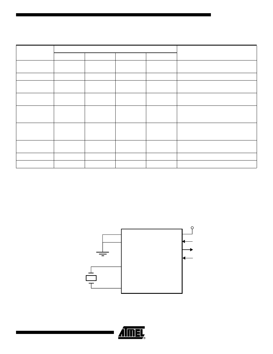
Figure 4. Serial Programming and Verify
Notes:
1. When
writing
, data is clocked on the
rising
edge of CLK.
2. When
reading
, data is clocked on the
falling
edge of CLK. See Figure 5 for an
explanation.
Table 6. AT86RF401 Serial Programming Instruction Set
Instruction
Instruction Format
Operation
Byte 1
Byte 2
Byte 3
Byte 4
Programming
Enable
1010 1100
0101 0011
xxxx xxxx
xxxx xxxx
Enable Serial Programming after
RESETB goes low.
Chip Erase
1010 1100
100x xxxx
xxxx xxxx
xxxx xxxx
Chip erase EEPROM
Read Program
Memory
0010 H000
0000 00aa
bbbb bbbb
oooo oooo
Read H (high or low) data o from Program
memory at word address a:b
Write Program
Memory
0100 H000
0000 00aa
bbbb bbbb
iiii iiii
Write H (high or low) data i to Program
memory at word address a:b
Read
EEPROM
Memory
1010 0000
0000 0000
xbbb bbbb
oooo oooo
Read data o from EEPROM memory at
address b
Write
EEPROM
Memory
1100 0000
0000 0000
xbbb bbbb
iiii iiii
Write data i to EEPROM memory at
address b
Write Lock Bits
1010 1100
111x x
21x
xxxx xxxx
xxxx xxxx
Write lock bits. Set bits 21 = “0” to
program lock bits.
I/O Read
10110000
0000 0000
00bbbbbb
oooo oooo
Read data 0 from I/O memory address b
I/O Write
11010000
0000 0000
00bbbbbb
iiii iiii
Write data i to I/O memory address b
BAT
SCK
SDO
SDI
RESETB
XTAL
XTALB
2.0–3.5V
CLOCK IN
DATA OUT
INSTR. IN, DATA IN
GND
6 to 20 MHz
AT86RF401