Avr core, Architectural overview – Rainbow Electronics AT86RF401 User Manual
Page 16
16
AT86RF401
1424D–RKE–09/02
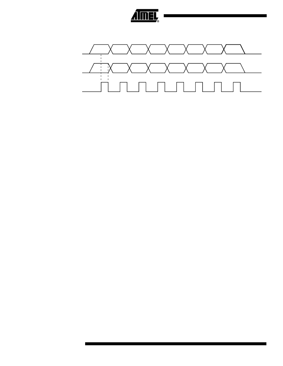
Figure 5. Serial Programming Waveforms
Note:
This device includes an integrated 128-byte EEPROM, which is accessed by three registers located in the I/O memory space.
These are the DEECR, DEEDR and DEEAR registers. For more information, refer to I/O Register Description.
AVR Core
Architectural Overview
The fast-access register file concept contains 32 x 8-bit general-purpose working regis-
ters with a single clock cycle access time. This means that during one single clock cycle,
one Arithmetic Logic Unit (ALU) operation is executed. Two operands are output from
the register file, the operation is executed, and the result is stored back in the register
file in one clock cycle.
Six of the 32 registers can be used as three 16-bit indirect address register pointers for
Data Space addressing, enabling efficient address calculations. One of the three
address pointers is also used as the address pointer for look-up tables in Flash program
memory. These added function registers are the 16-bit X-register, Y-register and Z-
register.
The ALU supports arithmetic and logic operations between registers or between a con-
stant and a register. Single register operations are also executed in the ALU. Figure 6
shows the AT86RF401 AVR architecture.
In addition to the register operation, the conventional memory addressing modes can be
used on the register file as well. This is enabled by the fact that the register file is
assigned the 32 lowest data space addresses ($00–$1F), allowing them to be accessed
as though they were ordinary memory locations.
The I/O memory space contains 64 addresses for CPU peripheral functions as Control
Registers, Timer/Counters, A/D converters and other I/O functions. The I/O Memory can
be accessed directly or as the Data Space locations following those of the register file,
$20–$5F.
SERIAL DATA INPUT (SDI)
SERIAL DATA OUTPUT (SDO)
SERIAL CLOCK INPUT (SCK)
MSB
MSB
LSB
LSB