Rainbow Electronics AT86RF401 User Manual
Page 27
27
AT86RF401
1424D–RKE–09/02
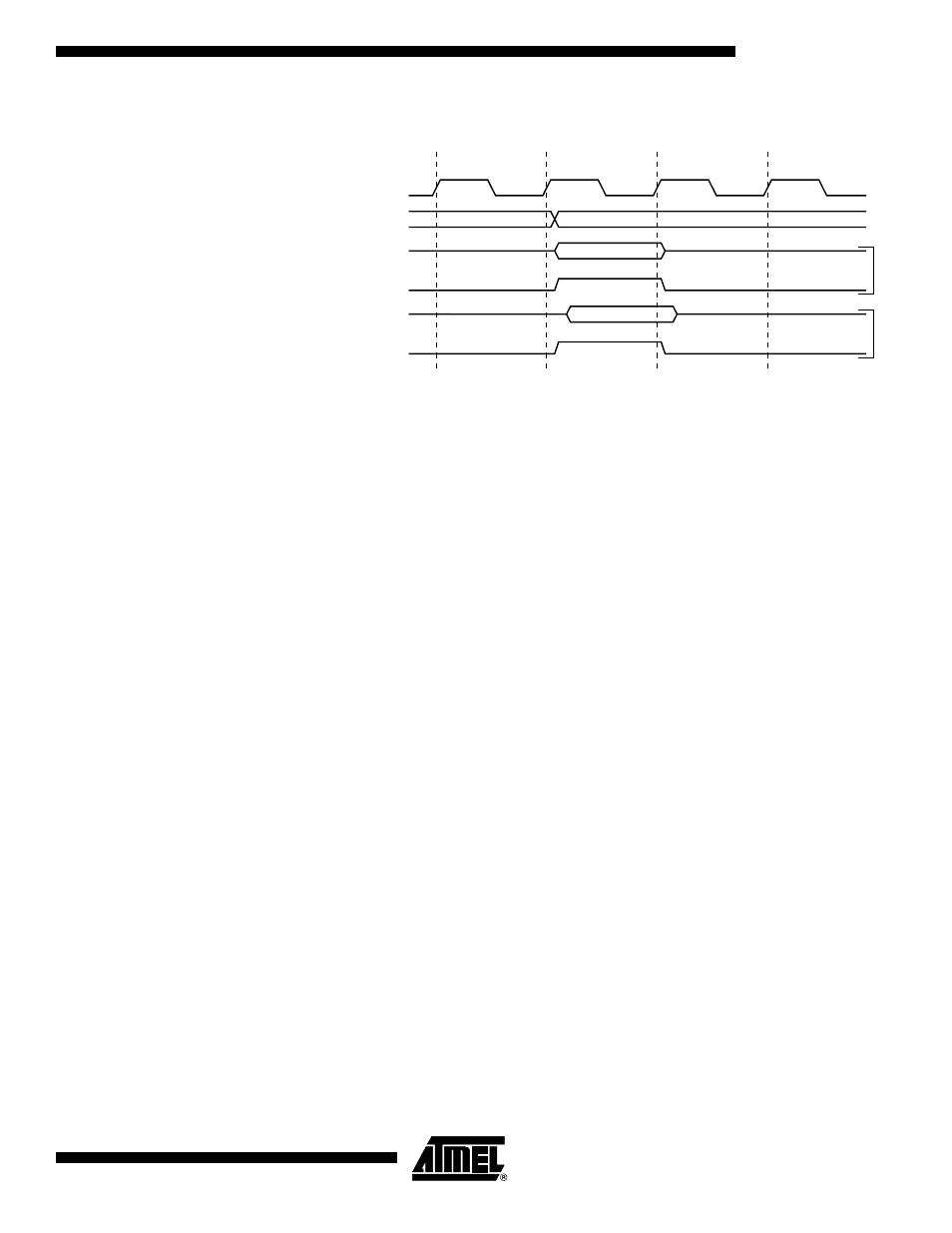
Figure 24. On-chip Data SRAM Access Cycles
All I/Os and peripherals are placed in the I/O space. The I/O locations are accessed by
the IN and OUT instructions, transferring data between the 32 general-purpose working
registers and the I/O space. I/O registers within the address range $00–$1F are directly
bit-accessible using the SBI and CBI instructions. In these registers, the value of single
bits can be checked by using the SBIS and SBIC instructions. Refer to Table 10,
“Instruction Set Manual,” on page 44 for more details. When using the I/O specific com-
mands IN and OUT, the I/O addresses $00–$3F must be used. When addressing I/O
registers as SRAM, $20 must be added to these addresses.
For compatibility with future devices, reserved bits should be written to “0” if accessed.
Reserved I/O memory addresses should never be written.
Some of the status flags are cleared by writing a logical “1” to them. Note that the CBI
and SBI instructions will operate on all bits in the I/O register, writing a “1” back into any
flag read as set, thus clearing the flag. The CBI and SBI instructions work with registers
$00 to $1F only.
The I/O and peripherals control registers are explained in the following sections.
System Clock Ø
Write
Read
Data
Data
Address
Address
T1
T2
T3
T4
Prev. Address
Read
Wr
ite