I/o and control registers, Transmitter control register descriptions, Lock detector configuration register 1 – lockdet1 – Rainbow Electronics AT86RF401 User Manual
Page 29
29
AT86RF401
1424D–RKE–09/02
I/O and Control
Registers
The AT86RF401 I/Os and peripherals are placed in the I/O space. The various I/O loca-
tions are accessed by the IN and OUT instructions transferring data between the 32
general-purpose working registers and the I/O space. I/O registers within the address
range $00–$1F are directly bit-accessible using the SBI and CBI instructions. In these
registers, the value of single bits can be checked by using the SBIS and SBIC instruc-
tions. Refer to Table 10 on page 44 for more details. The different I/O and peripherals
control registers are explained in the following sections.
Transmitter Control Register Descriptions
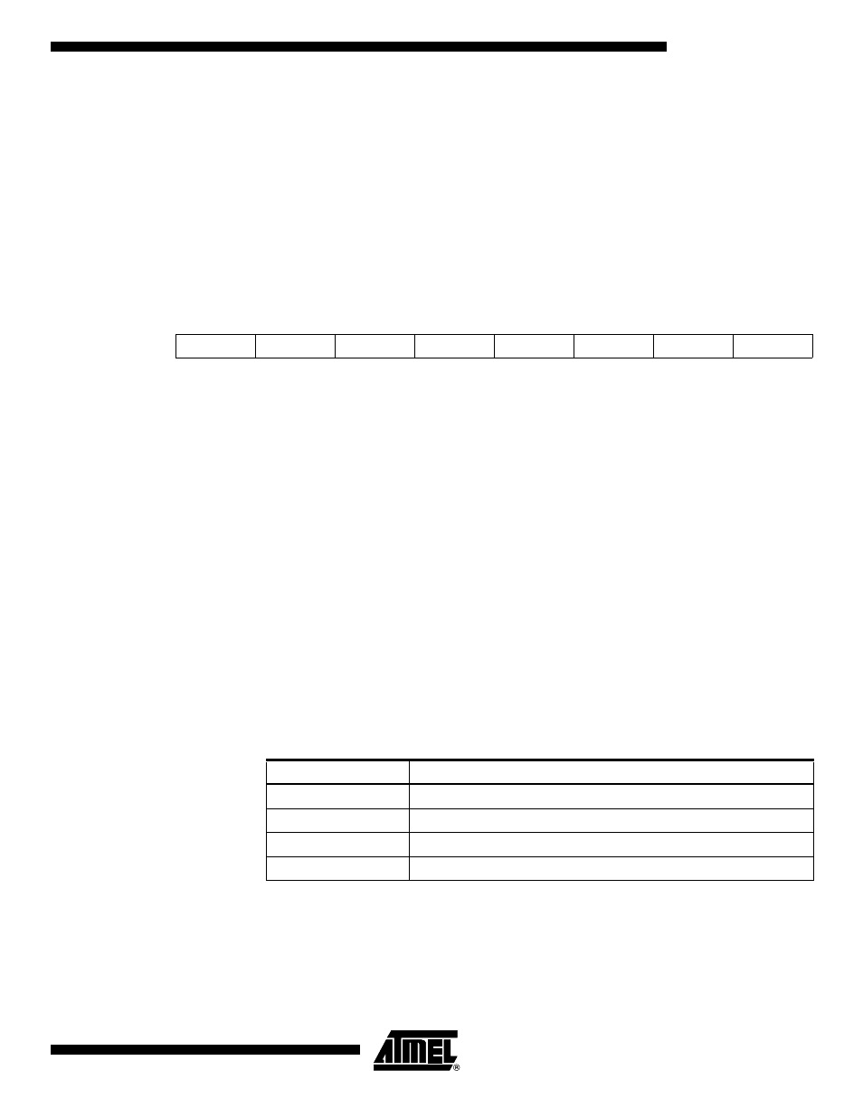
Lock Detector Configuration Register 1 – LOCKDET1
• Bits[7:5]
Reserved.
• Bit[4]: UPOK
If set high, this bit resets the unlock counter. The bit is level sensitive, and the unlock
counter will not count unless this bit is set to “0”. Leaving this bit high essentially dis-
ables the unlock detector.
• Bit[3]: ENKO (Enable Key on Bit)
If set to “1”, the rising edge of TXK starts the blackout period, during which any cycle
slips are ignored and do not affect the unlock circuit.
• Bit[2]: BOD (Black Out Disable)
When set high, cycle slips are counted immediately but only if LOCK is asserted high
(TX_CNTL b[2]).
• Bits[1:0] CS[1:0]: Cycle Slip Counter
These two bits determine how many cycle slips are allowed before the LOCKDETECT
signal is set low. The cycle slips are not counted unless the blackout logic is either dis-
abled or the blackout window has passed.
Bit
7
6
5
4
3
2
1
0
$10
–
–
–
UPOK
ENKO
BOD
CS1
CS0
Read/Write
R/W
R/W
R/W
R/W
R/W
R/W
R/W
R/W
Initial Value
0
0
0
0
0
0
0
0
CS[1:0]
Functionality
00
1 cycle slip causes unlock condition
01
2 cycle slips cause unlock condition
10
3 cycle slips cause unlock condition
11
4 cycle slips cause unlock condition