Footprint migration differences, Footprint, Migration differences – Xilinx DS610 User Manual
Page 99: E the, Footprint migration, Differences, Section f
Spartan-3A DSP FPGA Family: Pinout Descriptions
DS610 (v3.0) October 4, 2010
Product Specification
99
Footprint Migration Differences
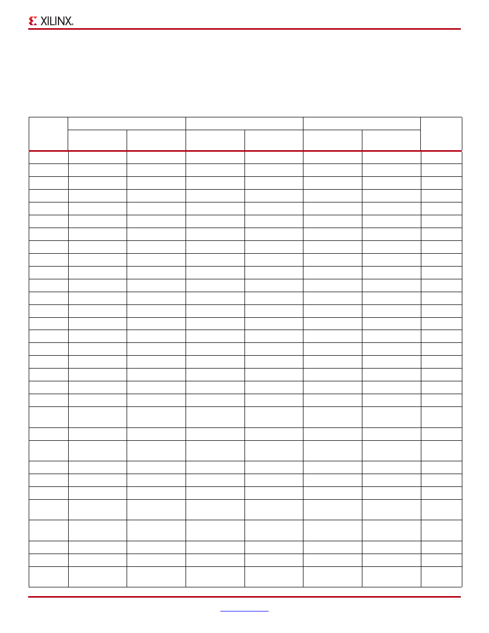
There are multiple migration footprint differences between the XC3SD1800A and the XC3SD3400A in the FG676 package.
These migration footprint differences are shown in
. Migration from the XC3S1400A Spartan-3A device in the
FG676 package to a Spartan-3A DSP device in the FG676 package is also possible. The XC3S1800A pin migration
differences have been added to
for designs migrating between these devices.
Table 70: FG676 Footprint Migration Differences
FG676
Ball
Spartan-3A
Spartan-3A DSP
Spartan-3A DSP
FG676
Ball
XC3S1400A
Type
XC3S1400A
Bank
XC3SD1800A
Type
XC3SD1800A
Bank
XC3SD3400A
Type
XC3SD3400A
Bank
G16
IP_0
0
IP_0
0
GND
GND
G16
G18
N.C.
N.C.
IP_0
0
VCCINT
VCCINT
G18
F9
N.C.
N.C.
IP_0
0
VCCAUX
VCCAUX
F9
F10
IP_0
0
IP_0
0
VCCINT
VCCINT
F10
F18
N.C.
N.C.
IP_0
0
VCCINT
VCCINT
F18
E6
N.C.
N.C.
IP_0
0
VCCINT
VCCINT
E6
E9
N.C.
N.C.
IP_0
0
GND
GND
E9
E20
IP_0
0
IP_0
0
VCCAUX
VCCAUX
E20
D5
N.C.
N.C.
IP_0
0
VCCINT
VCCINT
D5
D15
IP_0
0
IP_0
0
GND
GND
D15
D19
IP_0
0
IP_0
0
GND
GND
D19
C4
IP_0
0
IP_0
0
VCCINT
VCCINT
C4
B24
N.C.
N.C.
IP_0
0
GND
GND
B24
A5
IP_0
0
IP_0
0
GND
GND
A5
A7
IP_0
0
IP_0
0
VCCO_0
0
A7
A23
IP_0
0
IP_0
0
GND
GND
A23
A24
N.C.
N.C.
IP_0
0
VCCAUX
VCCAUX
A24
Y26
IP_L16N_1
1
IP_L16N_1
1
IP_1
1
Y26
W25
IP_L16P_1
1
IP_L16P_1
1
GND
GND
W25
W26
IP_L20P_1
1
IP_L20P_1
1
VCCAUX
VCCAUX
W26
V26
IP_L20N_1/
VREF_1
1
IP_L20N_1/
VREF_1
1
IP_1/VREF_1
1
V26
U25
IP_L24P_1
1
IP_L24P_1
1
GND
GND
U25
U26
IP_L24N_1/
VREF_1
1
IP_L24N_1/
VREF_1
1
IP_1/VREF_1
1
U26
H23
IP_L48P_1
1
IP_L48P_1
1
VCCAUX
VCCAUX
H23
H24
IP_L48N_1
1
IP_L48N_1
1
IP_1
1
H24
H25
IP_L44N_1
1
IP_L44N_1
1
VCCO_1
1
H25
H26
IP_L44P_1/
VREF_1
1
IP_L44P_1/
VREF_1
1
IP_1/VREF_1
1
H26
G25
IP_L52N_1/
VREF_1
1
IP_L52N_1/
VREF_1
1
IP_1/VREF_1
1
G25
G26
IP_L52P_1
1
IP_L52P_1
1
VCCAUX
VCCAUX
G26
B25
IP_L65N_1
1
IP_L65N_1
1
GND
GND
B25
B26
IP_L65P_1/
VREF_1
1
IP_L65P_1/
VREF_1
1
IP_1/VREF_1
1
B26