Phase shifter (ps), Miscellaneous dcm timing, Table 41 – Xilinx DS610 User Manual
Page 48
Spartan-3A DSP FPGA Family: DC and Switching Characteristics
DS610 (v3.0) October 4, 2010
Product Specification
48
Phase Shifter (PS)
Miscellaneous DCM Timing
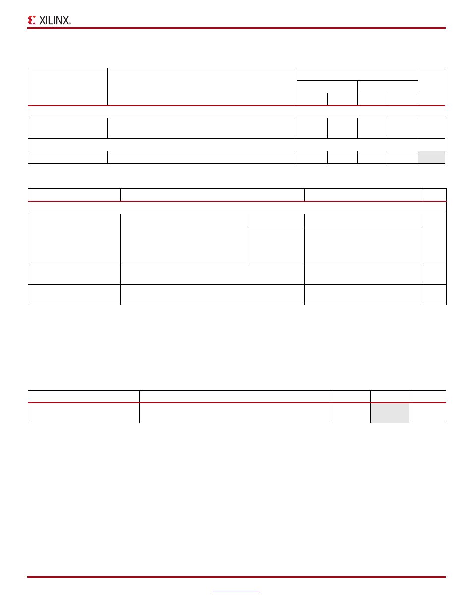
Table 40: Recommended Operating Conditions for the PS in Variable Phase Mode
Symbol
Description
Speed Grade
Units
-5
-4
Min
Max
Min
Max
Operating Frequency Ranges
PSCLK_FREQ
(FPSCLK)
Frequency for the PSCLK input
1
167
1
167
MHz
Input Pulse Requirements
PSCLK_PULSE
PSCLK pulse width as a percentage of the PSCLK period
40%
60%
40%
60%
–
Table 41: Switching Characteristics for the PS in Variable Phase Mode
Symbol
Description
Phase Shift Amount
Units
Phase Shifting Range
MAX_STEPS
Maximum allowed number of
DCM_DELAY_STEP steps for a given
CLKIN clock period, where T = CLKIN
clock period in ns. If using
CLKIN_DIVIDE_BY_2 = TRUE, double
the effective clock period.
CLKIN < 60 MHz
±[INTEGER(10 • (T
CLKIN
– 3 ns))]
steps
CLKIN
≥ 60 MHz
±[INTEGER(15 • (T
CLKIN
– 3 ns))]
FINE_SHIFT_RANGE_MIN
Minimum guaranteed delay for variable phase shifting
±[MAX_STEPS •
DCM_DELAY_STEP_MIN]
ns
FINE_SHIFT_RANGE_MAX Maximum guaranteed delay for variable phase shifting
±[MAX_STEPS •
DCM_DELAY_STEP_MAX]
ns
Notes:
1.
The numbers in this table are based on the operating conditions set forth in
and
Table 40
.
2.
The maximum variable phase shift range, MAX_STEPS, is only valid when the DCM is has no initial fixed phase shifting, that is, the
PHASE_SHIFT attribute is set to 0.
3.
The DCM_DELAY_STEP values are provided at the bottom of
Table 42: Miscellaneous DCM Timing
Symbol
Description
Min
Max
Units
DCM_RST_PW_MIN
Minimum duration of a RST pulse width
3
–
CLKIN
cycles